


Umicore Electroplating is introducing the IGEPIG process, developed by Uyemura, as its exclusive European distributor.
 Andreas GrossThe nickel-free final finish combines a gold seed layer, a palladium diffusion barrier, and a final gold top coat. The process is particularly suited for electronics applications that require high signal integrity, very narrow line spaces, or flexible copper substrates.
As frequencies rise and electronic assemblies continue to miniaturize, the choice of final finish is becoming even more important. Established plating systems such as ENIG (electroless nickel, immersion gold) and ENEPIG (electroless nickel, electroless palladium, immersion gold) include a nickel layer between the copper substrate and the outer precious metal coating. This layer serves as a diffusion barrier and a base for the subsequent layer structure. However, in certain high-frequency, fine-line, and flexible circuit applications, nickel can become a limiting factor.
Nickel-Free Layer Structure With a Palladium Diffusion Barrier
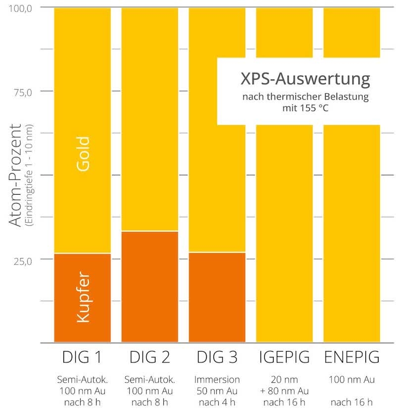 The XPS analysis following thermal exposure clearly shows that the palladium layer acts as a diffusion barrier in the nickel-free IGEPIG process.To provide the necessary functions without a nickel layer, the standard IGEPIG (Immersion Gold, Electroless Palladium, Immersion Gold) process combines a catalytically active, 20-nanometer-thick gold seed layer with a 100-nanometer-thick, chemically deposited palladium layer and a final 80-nanometer-thick gold top layer.
The gold seed layer provides the catalytic basis for homogeneous, controlled palladium deposition. The palladium layer acts as a diffusion barrier between copper and gold, preventing copper from diffusing into the functional gold layer. This is particularly important for final finishes exposed to thermal stress. The final gold top layer protects the underlying palladium and provides the properties for further processing.
High Frequency, Ultra-Fine Line Spaces and Flexible Copper Substrates
At high frequencies, nickel-containing intermediate layers can attenuate electrical signals due to nickel’s ferromagnetic properties. This effect becomes more significant as frequency increases, since the skin effect concentrates current on the conductor’s surface. For applications where minimizing transmission losses is critical, a nickel layer can therefore be a limiting factor.
The nickel-free structure also offers advantages for very fine line and space geometries. The IPC specifications 4552 for ENIG and 4556 for ENEPIG stipulate nickel layer thicknesses of three to six micrometers to ensure an effective diffusion barrier. As structures shrink, this nickel layer reduces the available spacing between neighboring lines. In addition, the activator system required for electroless nickel plating adds complexity. For line spaces of less than 50 micrometers, activator residues can cause footing or stray plating, thereby increasing the risk of short circuits. Since IGEPIG requires neither a nickel layer nor the associated activator system, these process-related risks can be reduced. To date, IGEPIG has been used to plate line spaces of less than 20 micrometers without stray plating or bridging.
The IGEPIG process can successfully coat line spaces under 20 µm.
Furthermore, eliminating the relatively low-ductility nickel layer makes IGEPIG a suitable final finish option for flexible copper substrates. Nickel can limit the mechanical flexibility of the plated copper. A nickel-free final finish is therefore also relevant for applications in which flexible copper surfaces must be reliably plated and subsequently subjected to mechanical stress.
Solder Joint Reliability and a Comparative Test
 The IGEPIG process can successfully coat line spaces under 20 µm.In addition to these application-specific advantages, the new layer structure must ensure the final finish's functional reliability. The solder joint reliability of IGEPIG was therefore evaluated using ball grid array (BGA) shear tests. Under the test conditions used, IGEPIG and the established ENEPIG system achieved the highest shear forces among the variants examined. This remained even after four hours of thermal exposure at 155 degrees Celsius. The results show that, under these test conditions, IGEPIG achieves solder joint reliability comparable to ENEPIG.
“With IGEPIG, we bridge the gap between simple nickel-free gold surfaces and the established ENEPIG system. Users receive a nickel-free final finish with a palladium diffusion barrier and can tailor the layer structure specifically to the electrical, geometric and thermal requirements of their application without compromising functionality,” says Andreas Gross, Division Manager PCB-Processes at Umicore Electroplating.
IGEPIG and DIG: a Gold Bath For Both Final Finishes
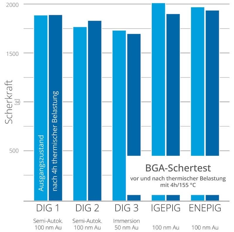 The BGA shear test shows that IGEPIG achieves solder joint reliability comparable to ENEPIG.However, not every application requires the additional palladium diffusion barrier provided by the IGEPIG system. For applications with lower thermal or functional requirements, DIG (Direct Immersion Gold) without a diffusion barrier may still be the technically and economically suitable, nickel-free solution. Umicore therefore combines both final coatings in a flexible 2-in-1 process concept.
A single gold bath supports three deposition steps: the gold seed layer and final gold top layer in IGEPIG, as well as direct gold deposition in DIG. This lets users choose between the two final finishes based on their requirements, without needing an additional gold bath for DIG.
Umicore Electroplating supports customers in the technical and economic evaluation as well as the implementation of IGEPIG. The offering includes test plating for initial investigations, application-specific economic analyses, consulting on the required process landscape and equipment technology, and support during process implementation. On this basis, it is possible to determine whether IGEPIG is the appropriate final finish for the respective application.