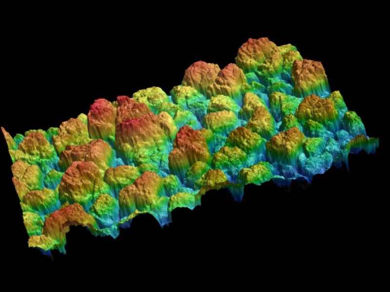
Due to its unique physical and chemical properties, bismuth is an attractive candidate for a wide range of applications such as battery anodes, radiation shielding, and semiconductors, to name a few.
This work presents the electrodeposition of mechanically stable and homogenous bismuth films at micron-scale thicknesses. A simple one-step electrodeposition process using either a pulse/reverse or direct current source yielded thick, homogenous, and mechanically stable bismuth films. Morphology, electrochemical behavior, adhesion, and mechanical stability of bismuth coatings plated with varying parameters were characterized via optical profilometry, cyclic voltammetry, electron microscopy, and tribology. Scratch testing on thick electroplated coatings (> 100 µm) revealed similar wear resistance properties between the pulse/reverse plated and direct current electroplated films. This study presents a versatile bismuth electroplating process with the possibility to replace lead in radiation shields with an inexpensive, non-toxic metal, or to make industrially relevant electrocatalytic devices.
Introduction
 Authors: top row, left to right, Nathan Brown, Enkeleda Dervishi, and Kendrich Hatfield; bottom row, Daniel Hooks, Don Johnson, and Genevieve C. Kidman. Not pictured: Courtney Clark.Bismuth is a semimetal with interesting physical, electrical, and chemical properties1,2. Its unique properties, low toxicity3, and availability lead to many applications, such as battery anodes4, semiconductors for electrocatalytic degradation of organic waste5, and superconductors6. Moreover, Bi has a high hydrogen evolution overpotential, allowing higher current efficiency for reductive processes in electrochemical devices, and it has a high electrocatalytic activity toward CO2 reduction7. Bi is also an effective radiation shielding material8,9 and has high magnetoresistance10, making it useful in a variety of other applications such as radiation safety and magnetic sensing. Several methods such as sputtering11, thermal evaporation12, molecular beam epitaxy13, and electrodeposition1,2,14 have been used to fabricate Bi films. Electrodeposition is particularly attractive, being amenable to mild temperature and pressure conditions on irregularly shaped substrates of a wide range of sizes, with great control over resulting surface morphology10. Previous studies have demonstrated electrodeposition of Bi, generally obtaining nanometer14 to single micron1,15 thicknesses. For some practical applications (particularly radiation shielding), thicker, robust films are desirable16. Millimeter-scale electrodeposited Bi coatings have been previously demonstrated a few times in literature on copper films16 and a nickel-phosphorous coating17 using constant current density deposition methods. However, pulsed electrodeposition is regularly employed to improve coating deposition and brightness18, and has been used before for thinner Bi coatings19. Possible benefits include a more dense and uniform coating due to the steeper concentration gradient at the surface, as well as better control over film morphology. This work demonstrates a simple, one-step process for depositing Bi films > 100 µm thick with subsequent examination of the effects of pulsed vs direct current plating, differing current densities, and deposition time. Coatings were characterized via electron microscopy, cyclic voltammetry, and tribology to fully understand their structure, adhesion, and mechanical stability.
Materials and Electrodeposition
Electrodeposition
Potassium hydroxide (VWR, reagent grade), tartaric acid (Acros organics, 99+%), bismuth (III) nitrate pentahydrate (either Alfa Aesar, 98% or Acros organics, 99.999%), glycerol (VWR, biotechnology grade), and nitric acid (Millipore-Sigma, Emplura, 65%) were used as received for electrodeposition. The plating solution consisted of bismuth nitrate (0.15 M), glycerol (1.4 M), KOH (1.2 M), tartaric acid (0.33 M), and HNO3 to adjust pH, which was measured with a Thermo Scientific Orion Star A221 pH meter equipped with a Thermo Scientific 9107BNMD triode. A Dynatronix DuPR10-3-6XR power supply was used with a two-electrode configuration: platinized titanium as an anode/counter electrode (CE) and a gold-plated brass or steel panel (5 µm thick) as the cathode/working electrode. The electrodes were suspended in a glass beaker filled with the plating solution with a magnetic stir bar over a stir plate for all electrodeposition processes. All experiments were performed at room temperature.
Bismuth film analysis
An Apreo 1 or 2 SEM with an EDAX or Oxford EDS attachment was used for SEM characterization including electron backscatter diffraction (EBSD). Apex OIM software was used to analyze EBSD data. Accelerating voltage for all SEM images was 20 kV. An SP-300 Biologic potentiostat was used with a 3-electrode configuration with a standard calomel reference electrode (saturated KCl), a carbon rod CE, and electrodeposited bismuth working electrode to test hydrogen evolution reaction (HER) on electroplated bismuth in 10% HNO3. An RTEC MFT-5000 tribometer was used with a Rockwell type C tip for progressive load scratch testing from 0.1 to 40 N. Prior to tribological tests, Bi films were polished with 10–12 µm (800 grit) sandpaper. A Keyence VK-1000X optical profilometer was used to image films for roughness and assess wear volumes for tribological scratch tests.
XRD was performed on a Rigaku Ultima III diffractometer with fine line sealed Cu tube Kα (λ = 1.5406 Å) x-rays and a D/MAX Ultima series with a maximum power of 3 kW. XRD data was collected on a continuous scan mode in Bragg–Brentano slit geometry over a 2-theta range of 5°–90° with sampling width of 0.05° and scanning speed of 1.5°/min. The divergence slit was set to 2.0 mm, the divergence H.L. slit was set at 10 mm, and the scattering and receiving slits were set to open and open.
Results and Discussion
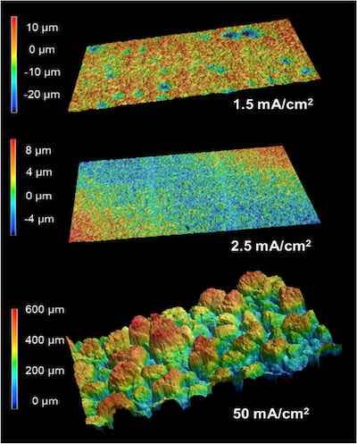 Figure 1. Optical profilometry of intact Bi films electrodeposited at 50 mA/cm2, 2.5 mA/cm2, and 1.5 mA/cm2.Understanding the effects of electrodeposition parameters
Many parameters profoundly affect Bi electroplating, making proper conditions paramount to obtaining a film with homogenous surface coverage and good adhesion. In addition to Bi(NO3)3, we added tartaric acid and glycerol as chelating agents in the same manner as Chen et al.15 to help moderate film growth10 and stabilize Bi3+ ion. Plating in this solution is highly sensitive to solution pH, with the best coating obtained at a pH range of 0.01–0.1, resulting in a robust film, while higher pH values produce a film with poor adhesion, able to be wiped away easily by hand. For all further experiments, we adjusted the pH to ~ 0.08 with HNO3 before plating. Current density was found to significantly affect film quality; samples plated with current densities of 180 mA/cm2 and 50 mA/cm2 had inconsistent topographies, with Sa values generally greater than 50 µm and poor adhesion, often delaminating from the substrate upon removal from the electrolyte. Thus, we used a current density of 1.5 mA/cm2 for later experiments. Figure 1 shows optical profilometry and photos of intact films grown with direct currents of 50 mA/cm2 for 17 h, 2.5 mA/cm2 for 24 h, and 1.5 mA/cm2 for 24 h. Sandnes et al. reported that current densities above 10 mA/cm2 resulted in significantly rougher films1, agreeing with our results. Current densities of 1.5 mA/cm2 (Sa of 5.2 µm) and 2.5 mA/cm2 (Sa of 2.6 µm) yielded the brightest and smoothest films.
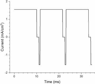 Figure 2. Waveform of the current-controlled pulsed plating process. Both the reverse and forward pulses were 1.5 mA/cm2.Pulsed and direct current electrodeposited bismuth
Many researchers have used pulsed electrodeposition with a variety of pulse waveforms to obtain more uniform films, higher plating efficiency, and control over morphologies and grain sizes20. Pulses used range from sub-millisecond to second timescales and can include “reverse” pulses (i.e. a stripping current) which can improve film uniformity20. While a full study of different pulse sequences is beyond the scope of this article, we tested Bi electrodeposition using a pulse/reverse plating process with millisecond-scale pulses (waveform shown in Fig. 2) and compared the resulting coatings with those obtained with direct current plating.
We used a current density of 1.5 mA/cm2 for both pulsed and DC depositions and plated samples for 24 and 96 h. Figure 3 shows SEM images of each sample. The DC-plated samples both show elongated features on the surface, with those on the 96-h DC sample being very thin. On the other hand, the pulse-plated samples displayed a mixed morphology with regions of both elongated features like the 24-h DC sample and “blockier” morphologies with features roughly 2–5 µm in diameter, similar to those found by Gades, et al.21. This implies that the electrodeposition waveform has an effect on surface morphology which in turn has been shown to affect electrocatalytic properties19. We also observed grains with EBSD on polished cross-sections of 96-h plated samples and estimated grain sizes of 19 µm for the DC-plated coating and 41 µm for the pulse-plated coating (Fig. 4, size histogram in Figure S1). Generally, pulse-plating leads to finer grains than direct current22, but our results for the DC-plated grains are likely skewed by the high presence of suspected twinning. Overall, our results indicate that this electrodeposition method offers control over film microstructure, which can significantly impact the physical properties of metals23.
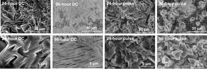 Figure 3. Scanning electron microscopy (20 kV accelerating voltage) of electroplated bismuth at various magnifications.
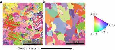 Figure 4. EBSD of 96-h (a) DC-plated and (b) pulse-plated bismuth coatings.We measured film thicknesses (summarized along with deposition rate and deposition efficiency in Table 1) by cross-sectional SEM (Figure S2); thicknesses varied widely for the 24-h pulse/reverse and DC-plated samples, from 80 to 290 µm. As other have previously noted, film thickness is heavily affected by hydrodynamics (i.e. stirring/bath geometry) and cathode placement24,25, though the majority of our films were ≥ 100 µm. The 96-h electroplated samples had more consistent thicknesses with DC-plating yielding thicker films than pulsed-plating, likely due to the lower effective current (i.e. duty cycle) of the pulse sequence. These results indicate that either pulsed or DC electroplating is effective to obtain thick (> 100 µm) Bi films with good coverage at high deposition efficiencies (> 70%).
Table 1 Electrodeposition results.
| Deposition parameters | Coating thickness (µm) | Deposition rate (µm/h) | Deposition efficiency (%) |
| 24-h DC | 80–290 | 3.3–12 | 98 |
| 96-h DC | 330–500 | 3.6–5.1 | 72 |
| 24-h pulse | 90–260 | 4.0–10.6 | 91 |
| 96-h pulse | 230–320 | 2.5–3.1 | 83 |
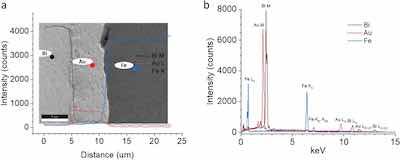 Figure 5. EDS of a bismuth-plated sample cross-section. (a) Linescan data across the cross-section from the bismuth M line (black), gold L line (red), and iron K line (blue). (b) Overlaid EDS spectra of bismuth (black), gold (red), and iron (blue) areas in the cross section.An EDS linescan of a Bi-plated cross-section (96-h pulse-plated) shows clear separation between the bismuth, gold, and steel layers on the panel (Fig. 5a). Figure 5b shows overlaid individual EDS spectra of these regions. All samples showed comparable EDS results, shown in Figure S3, and Figure S4 shows an EDS map evidencing a homogenous Bi coverage on the sample surface.
We also performed XRD on a polished Bi surface (24-h pulse-plated) that matches that for Bi (Fig. 6)26,27.
Electrochemical testing
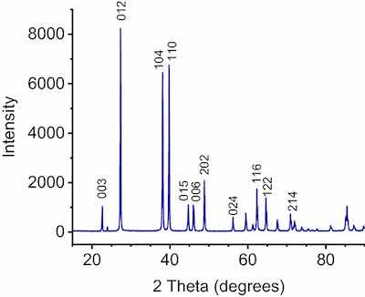 Figure 6. XRD of a polished 24-h pulse-plated Bi coating.To test the HER activity of electroplated Bi, a critical parameter in electrocatalytic applications, we performed cyclic voltammetry at 20 mV/s on 24-h pulse- and DC-plated bismuth films and plain gold in 10% HNO3. Figure 7 shows the higher overpotential of HER on Bi vs Au in the overlaid voltammograms. This is in agreement with Sandnes, et al.1, and indicates sufficient coverage of Bi to isolate gold from the solution. The pulse-plated sample yielded lower overpotentials for HER as compared to the DC sample, implying a difference in electrocatalytic activity between the two. This shows promise for electrochemical tunability based on electrodeposition parameters.
Hydrogen evolution reaction on 24-h pulse- and DC-plated bismuth compared to gold. Cyclic voltammetry performed at 20 mV/s in 10% HNO3 using a standard calomel reference electrode (saturated KCL) and a carbon rod counter electrode.
Mechanical properties
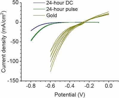 Figure 7. Hydrogen evolution reaction on 24-h pulse- and DC-plated bismuth compared to gold. Cyclic voltammetry performed at 20 mV/s in 10% HNO3 using a standard calomel reference electrode (saturated KCL) and a carbon rod counter electrode.Mechanically robust films are required for practical applications of these films such as radiation shields. We used progressive load scratch testing from 0.1 to 40 N to evaluate tribological performance via the critical load of failure characterized by delamination of the coating from the substrate in the form of gross spalation (Fig. 8-at least 3 scratch tests per sample)28. On the thinner 24-h plated samples (~ 100 µm), the scratch stylus broke through the Bi at 25 N for both pulse and DC-plated samples, exposing gold, but without substantial delaminating or cracking of the surrounding bismuth film. Figure 8 demonstrates the EDS maps of the scratch test area for the pulse-plated Bi films at various times. The thicker samples (< 200 µm) withstood up to 40 N (the force limit on our scratch measurement setup) without breaking through to the gold. The wear volume of the scratches, as measured by an optical profilometer, on the 96-h DC plated film were 0.029 ± 0.011 mm3, while the wear volume for the 96-h pulse plated sample were 0.035 ± 0.011 mm3, indicating similar resistance to scratching between the two plating methods. These results are evidence for good adhesion of the Bi to the Au and robustness for radiation shielding applications regardless of pulse waveform.
Conclusions
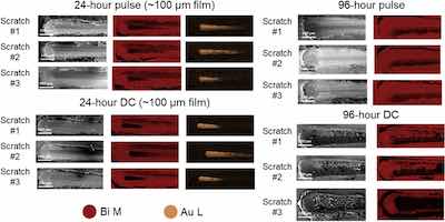 Figure 8. EDS maps of pulse-plated Bi films showing film breakthrough on ~ 100 μm 24-h samples, but not 96-h samples. Maps were made using Bi M lines and Au M lines.In this study, we demonstrated a simple, non-toxic process for electrodepositing thick (> 100 µm) Bi films on gold substrates and evaluated the effects of deposition time and pulsed vs DC electroplating. Increasing deposition times with both constant current and pulse/reverse methods lead to thicker films, showing potential for industrially usable, robust films for radioactive shielding applications. EDS showed a relatively pure and homogenous distribution of Bi throughout the film regardless of deposition parameters with a current density of 1.5 mA/cm2. Pulsed electrodeposition impacts surface morphology, grain size, and electrocatalytic activity of the electrolyte. Cyclic voltammetry showed higher HER activity on a pulse-plated sample compared to a DC-plated coating, implying a tunability for practical electrochemical applications. Mechanical strengths of DC- and pulse-plated coatings were similar, with scratch testing showing complete breakthrough of thin 24-h plated samples at 25 N with a Rockwell tip without excessive cracking or delamination. Scratch testing on samples > 200 µm also revealed similar wear resistance properties between DC and pulse plated films. Due to the versatility of electroplating toward substrates of irregular shapes and sizes, this study demonstrates a practical method of replacing lead in radiation shields with an inexpensive, non-toxic metal or for making industrially relevant electrocatalytic devices. Future experiments could involve testing films of varying thicknesses in a radioactive shielding environment or for carbon dioxide reduction to evaluate optimal Bi coating parameters for these applications.
Authors
Kendrich O. Hatfield1, Enkeleda Dervishi1*, Don Johnson1, Courtney Clark1, Nathan Brown1, Genevieve C. Kidman1, Darrick J. Williams2 and Daniel E. Hooks1,2
- SIGMA-2: Finishing Manufacturing Science, Los Alamos National Laboratories, SM-30 Bikini Atoll Road, Los Alamos, NM 87545, USA.
- MPA-CINT: Center for Integrated Nanotechnologies, Los Alamos National Laboratories, Los Alamos, NM 87544, USA.
*email: enkeleda@lanl.gov
Contributions: K.H.: Writing—original draft, Methodology, Formal analysis, Writing—review and editing. E.D.: Conceptualization, Investigation, Methodology, Formal analysis, Writing—review and editing. D.J.: Carried out the experiments, Investigation, Methodology. C.C.: Material Characterization and preparation N.B.: Material Characterization and preparation. G.K.: Grain size characterization and discussion of results. D.W.: XRD characterization and discussion. D.E.H.: Conceptualization, Methodology, Writing—review and editing.
References
- Sandnes, E., Williams, M. E., Bertocci, U., Vaudin, M. D. & Stafford, G. R. Electrodeposition of bismuth from nitric acid electrolyte. Electrochim. Acta 52, 6221–6228 (2007).
- Yang, M. & Hu, Z. Electrodeposition of bismuth onto glassy carbon electrodes from nitrate solutions. J. Electroanal. Chem. 583, 46–55 (2005).
- Keogan, D. M. & Griffith, D. M. Current and potential applications of bismuth-based drugs. Molecules 19, 15258–15297 (2014).
- Zhang, R., Bao, J., Wang, Y. & Sun, C. Concentrated electrolytes stabilize bismuth-potassium batteries. Chem. Sci. 9, 6193–6198 (2018).
- Meng, X. & Zhang, Z. Bismuth-based photocatalytic semiconductors: Introduction, challenges and possible approaches. J. Mol. Cat. A Chem. 423, 533–549 (2016).
- Sato, K. et al. Bismuth superconducting wires and their applications. Cryogenics 33(3), 243–246 (1993).
- Abdallah, R. et al. New porous bismuth electrode material with high surface area. J. Electroanal. Chem. 839, 32–38 (2019).
- Elsafi, M., El-Nahal, M. A., Sayyed, M. I. & Abbas, M. I. Novel 3-D printed radiation shielding materials embedded with bulk and nanoparticles of bismuth. Sci. Rep. 12, 12467 (2022).
- Wang, B., Ting, C., Lai, C. & Tsai, Y. Bismuth pelvic X-ray shielding reduced radiation dose exposure in pediatric radiography. Biomed. Res. Int. 2021, 9985714 (2021).
- Jiang, S., Huang, Y., Luo, F., Du, N. & Yan, C. Synthesis of bismuth with various morphologies by electrodeposition. Inorg. Chem. Commun. 6, 781–785 (2003).
- Stanley, S. A. & Cropper, M. D. Structure and resistivity of bismuth thin films deposited by pulsed DC sputtering. Appl. Phys. A 120, 1461–1468 (2015).
- Kumari, L. et al. Effects of deposition temperature and thickness on the structural properties of thermal evaporated bismuth thin films. Appl. Surf. Sci. 253, 5931–5938 (2007).
- Chen, T. et al. Stabilizing lithium metal anode by molecular beam epitaxy grown uniform and ultrathin bismuth film. Nano Energy 76, 105068 (2020).
- Prados, A. & Ranchal, R. Electrodeposition of Bi films on H covered n-GaAs(111)B substrates. Electrochim. Acta 305, 212–222 (2019).
- Chen, J. et al. Electroplating deposition of bismuth absorbers for X-ray superconducting transition edge sensors. Materials 14, 7169 (2021).
- Tishkevich, D. I. et al. Functional Bi coatings as a perspective material for radiation shields production against electron radiation. Adv. Mater. Lett. 11(2), 20021479 (2020).
- Cybul'skaja, L. S.; Poznjak, S. K.; Perevoznikov, S. S.; Shendjukov, V. S.; Gaevskaja, T. V.; Grabchikov, S. S.; Tishkevich, D. I. Method for applying a thick-layer bismuth coating to aluminium and alloys thereof for manufacture of radiation screens. 2017.
- Paunovic, M. Electrochemical aspects. In Modern Electroplating. Electrochemical Society Series 4th edn (eds Schlesinger, M. & Paunovic, M.) (Wiley, 2000).
- Park, J. Y. et al. The effect of pulse electrodeposition of bismuth on electrochemical reduction of carbon dioxide to formate. Electron. Mat. Lett. 15, 454–461 (2019).
- Devaraj, G., Guruviah, S. & Seshadri, S. K. Pulse plating. Mater. Chem. Phys. 25, 439–461 (1990).
- Gades, L. M. et al. Development of thick electroplated bismuth absorbers for large collection area hard X-ray transition edge sensors. IEEE Trans. Appl. Supercond. 27(4), 2101105 (2017).
- Karimi, S. & Foulkes, F. R. Modeling the effects of different pulse current waveforms on grain size of electrodeposited nickel coatings. J. Electrichem. Soc. 159(11), D659–D670 (2012).
- Armstrong, R. W. The influence of polycrystal grain size on several mechanical properties of materials. Metall. Mater. Trans. B 1, 1169–1176 (1970).
- Tan, Y. & Lim, K. Y. Understanding and improving the uniformity of electrodeposition. Surf. Coat. Technol. 167, 255–262 (2003).
- Yang, G., Deng, D., Zhang, Y., Zhu, Q. & Cai, J. Numerical optimization of electrodeposition thickness uniformity with respect to the layout of anode and cathode. Electrocatalysis 12, 478–488 (2021).
- Lafuente, B., Downs, R. T., Yang, H. & Stone, N. The power of databases: The RRUFF project. In Highlights in Mineralogical Crystallography (eds Armbruster, T. & Danisi, R. M.) 1–30 (De Gruyter, 2015).
- Sathiyaraj, P. & Samuel, E. J. J. Application of bi-nanoparticle on dose enhancement effect in two different polymer gel dosimeter using spectrophotometer. J. Can. Res. Ther. 14(3), 662–665 (2018).
- ASTM International. Standard Test Method for Adhesion Strength and Mechanical Failure Modes of Ceramic Coatings by Quantitative Single Point Scratch Testing; ASTM C1624–05 (2010).
Acknowledgements
The authors acknowledge the Laboratory Directed Research and Development (LDRD) funding programs at the Los Alamos National Laboratory for partially funding this work. This work was performed, in part, at the Center for Integrated Nanotechnologies, an Office of Science User Facility operated for the U.S. Department of Energy (DOE) Office of Science.
Ethics declarations
The authors declare no competing interests.
Additional information
Supplementary Information The online version contains supplementary material available at https://doi.org/10.1038/s41598-023-28042-z Correspondence and requests for materials should be addressed to E.D.


