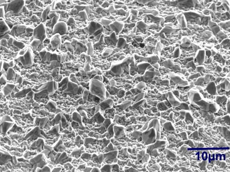
As RoHS lead free regulations began to take hold globally, tin and its alloys were the first choice as an alternative to eutectic tin/lead.
On the solder side the transition has moved forward and solutions have been implemented, like the Sn-Ag-Cu (SAC) family of lead-free (LF) solders, for paste reflow and tin/copper for HASL (hot air solder leveling). The industry is constantly making progress adapting its materials and processes to the higher reflow temperature profile for these LF solders. Today there is a much better understanding of the nature of the intermetallic (IMC) bond as well as the reliability of LF solder joint.
On the surface finish side, replacing tin/lead has posed greater challenges. Component leads and connector finishes were being converted to tin as an obvious alternative. This works well as a soldering surface, however any part of the lead or the connection surface that is not soldered to, has shown a potential to form tin whiskers over the life of the part. Internal stresses in the deposit due to IMC formation or external stresses on the deposit are known to initiate whisker formation.
In this paper two approaches are implemented to dissipate the stress that is formed. The first is to modify the substrate surface to control the growth in thickness and direction of propagation of the IMC. The second is to modify the large columnar tin deposit crystal structure to mimic the fine equiaxed structure of tin/lead solder. The former is achieved by controlled micro-roughening of the substrate and the latter by the use of additives to the plating bath. Data is presented showing that by implementing these two modifications that the stress causing tin whiskers is dissipated and tin whisker formation is inhibited.
Introduction
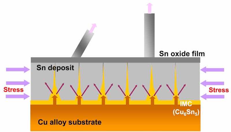 Figure 1 - A schematic diagram of tin whisker formation.Electroplated pure tin and tin-based alloys are being used as alternatives to tin/lead in the majority of electronic components. These alternatives are known to produce tin whiskers resulting in short circuits on these components.
In the case of a tin finish on copper and copper based alloys, the major cause of tin whisker formation is compressive stress. The stress is mainly caused by irregular growth of copper-tin intermetallic compound (IMC) at ambient conditions.
It is known that tin whiskers are readily formed on electroplated tin deposits on copper and are not observed on electroplated tin/lead deposits. The tin deposit and tin-lead deposit differ in crystal structure. The crystal structure has a direct impact on tin whisker formation.
A tin deposit with a modified crystal structure (similar to tin-lead deposits) is capable of preventing whisker formation by dissipating and delocalizing the stress that causes whiskers.
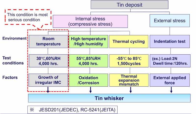 Figure 2 - The four different paths leading to stress and whisker formation.As shown in Fig. 1, stress channeled along the boundaries of the large grained columnar tin deposit, is responsible for the emergence of tin whiskers. Stress may be internal or external (Fig. 2). The primary source of internal stress is attributed to the non-uniform increase in the thickness of the intermetallic compound (IMC) layer over time at ambient conditions (30°C, 60% RH for 4000 hr). Another condition that produces internal stress is exposure to high temperature and high humidity (55°C, 85% RH for 4000 hr) for extended periods of time which gives rise to oxidation and/or corrosion. Internal stress can also be induced by thermal cycling (-55°C to 85°C; 1500 cycles) via mismatched coefficients of thermal expansion (CTE). The latter two forms are commonly used to induce internal stress in controlled experiments. External stress is also known to initiate whisker growth. An example is the stress induced by press fit connectors.
 Figure 3 - Test vehicle.
The approach taken in this study was to control the thickness of the IMC, as well as modifying the crystal structure of the tin deposit from large grained columnar structure to a small grain equiaxed one. The former is achieved by increasing the area of the copper substrate, by a chemical micro-roughening process. The grain structure is altered by the use of specific chemical additives to the plating bath. All testing was done under ambient conditions as noted above.
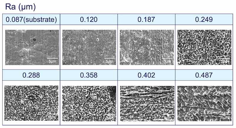 Figure 4 - SEM micrographs of plated surfaces exhibiting different Ra values.
Copper Surface Modification
 Figure 5 - The plating process sequence used for this study.A study was conducted on the morphology of the copper substrate prior to plating. A series of substrates varying in roughness were evaluated for whisker formation after electroplated tin deposition. The test vehicle used, as shown in Fig. 3, consisted of a CDA19400 lead frame (Composition: Cu-2.3 Fe-0.03 P-0.12 Zn).
The roughness was controlled by chemical etching procedures. The average roughness Ra, varied between 0.13 to 0.47 μm. As shown in Fig. 4, 0.47 μm Ra has a much larger surface area as compared to 0.13 μm Ra. The propensity to whisker was evaluated as follows:
Tin plating: The plating bath was an MSA-based matte tin solution. The plating was run at a current density of 10 A/dm2. The plating time was varied to produce a 3-μm and a 10-μm-thick deposit. The former was for short term whisker evaluation and the latter, typical of lead frame plating, was used for long term evaluations.
Methodology: The test vehicles were subjected to chemical micro-roughening to produce a set of specific Ra values (Fig. 4). The figure shows the SEM micrographs of the different degrees of micro-roughening, Ra, expressed in microns (μm). The samples were then run through a standard plating process as outlined in Fig. 5. They were then stored under controlled ambient conditions (30°C; 60% RH) for extended periods of time (1000 hr). The samples were examined for whisker formation at various time intervals.
Definition of a “whisker”: A whisker is a protrusion that is >10 μm in length and has an aspect ratio >2.
Measurement of whisker length: The measurement according to JEITA ET-7410 is the straight line distance from the point of emergence of the whisker to the most distant point on the whisker.
Results and Discussion
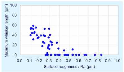 Figure 6 - Maximum whisker length versus surface roughness (1000 hr at 30°C; 60% RH).The whiskers were examined, measure and tabulated after 1000 hr of storage under controlled ambient conditions (30°C; 60% RH). The data gathered from whisker examination for the various surface roughness morphologies are plotted in Figs. 6 and 7.
Figure 6 illustrates maximum whisker length as a function of roughness. Figure 7 considers the whisker density per mm2 as a function of roughness. The data clearly indicate that there is clear correlation between surface roughness and whisker propensity. The rougher surface produces a lower whisker length and a lower whisker density. Figure 8 shows the whisker growth on 3 μm of tin plated on the smoother copper (Ra = 0.13 μm) compared with a rougher surface (Ra = 0.47 μm) exhibiting no whisker growth.
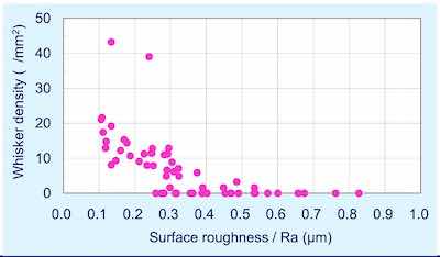 Figure 7 - Whisker density versus surface roughness (1000 hr at 30°C; 60% RH).In an effort to explain the mechanism of these observations, additional work was done. The 10-μm tin samples that were stored for 7000 hr at 30°C; 60% RH, were subjected to stripping of the tin by chemical means and the IMC morphology was examined. In addition, cross sections were prepared and examined to verify the top down observation.
Figure 9 shows the top view of the IMC after tin stripping on two extremes of Ra, namely Ra = 0.13 μm and Ra = 0.47 μm. Figure 10 shows deposit cross-sections for the same Ra values. It is clear that the higher Ra of 0.47 μm produced a thinner, more uniform IMC, compared to the smoother Ra of 0.13 μm, which showed increased IMC thickness in localized areas. A plausible explanation is that the IMC is spread over a much larger area on the rougher morphology (Ra = 0.47 μm) as compared to the smaller area of the smoother surface (Ra = 0.13 μm). It follows then that the stress resulting from IMC formation would be highly reduced and dissipated with increased surface roughness of the underlying copper substrate.
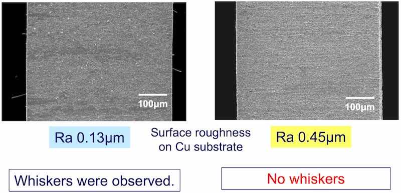 Figure 8 - The effect of surface roughness for 3 μm of tin (1000 hr at 30°C; 60% RH): (a) Ra = 0.13 μm, showing whisker growth and (b) Ra = 0.47 μm, showing no whisker growth.
The solderability and ductility of a 10-μm tin deposit on the two extremes of surface morphology were examined using “wetting balance testing” as well as the “bend test.” There was virtually no difference in performance, as seen in Fig. 11.
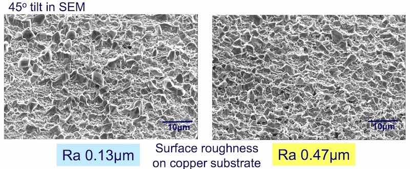 Figure 9 - Morphology of IMC surface after tin stripping: (a) Ra = 0.13 μm; (b) Ra = 0.47 μm.
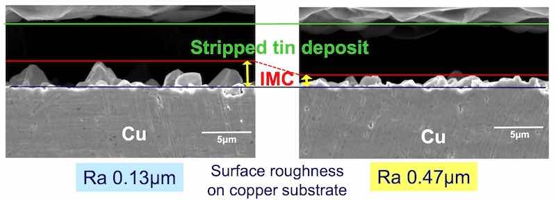 Figure 10 - Cross section showing the IMC after tin stripping: (a) Ra = 0.13 μm; (b) Ra = 0.47 μm.
Modifying the Crystal Structure of the Tin Deposit
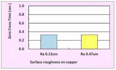 Figure 11 - Comparison of zero cross time of a 10-μm tin deposit for two levels of roughness.A close examination of the crystal structure of both the tin and Sn/Pb alloy shows a clear difference between the two deposits. The Sn/Pb alloy, which does not yield whiskers, has an equiaxed, relatively fine grained deposit. Tin, on the other hand, shows larger columnar crystals. Fig. 12 shows the difference in crystal structure between tin and the eutectic Sn/Pb alloy.
It is postulated that if the crystal structure of the tin deposit could be modified to the Sn/Pb crystal structure, the stresses would be dissipated and whiskers will not form. Tests were conducted using the same test vehicle and the same plating conditions as outlined earlier in the copper surface roughness study.
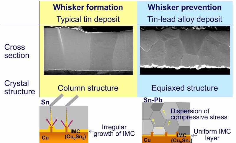 Figure 12 - SEM and schematic diagrams of the tin and Sn/Pb deposit structures, showing the stress distribution determined by the deposit structure.
Three types of tin deposits were produced by the use of specific plating additives to the bath. Type A is a standard tin deposit characterized by large columnar crystals, type B is modified to produce a smaller columnar grain structure, while type C was modified to produce a still smaller grain that is both columnar as well as equiaxed, essentially mimicking the Sn/Pb structure. The cross-sections and surface morphology of the three types of tin deposits are shown in Fig. 13.
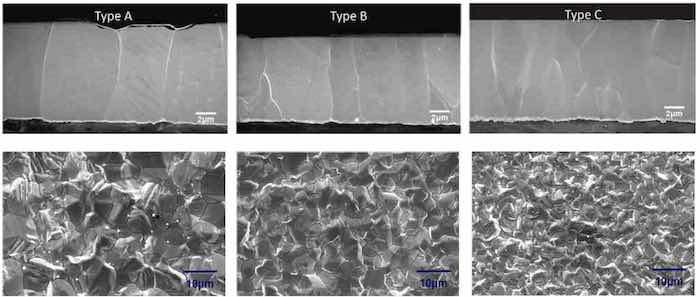 Figure 13 - SEM of the cross-section and surface morphologies in the three types of tin deposits.
 Figure 14 - Whisker growth characteristics exhibited by the three types of electrodeposited tin under study: Type A, long whiskers; type B, shorter whiskers and type C, no whisker growth.
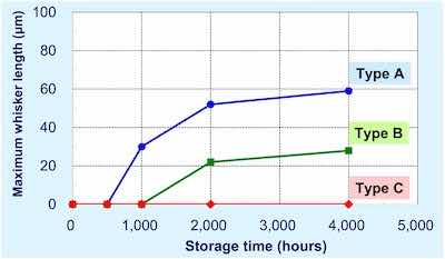 Figure 15 - Storage time versus maximum whisker length for the three types of tin structures.All three types were plated to the typical thickness of 10 μm (thickness typical of lead frames) and were placed in an ambient environment (30°C; 60% RH) for 4000 hr. Figure 14 shows the whisker formation behavior of the three types of electrodeposited tin. The type A tin deposit developed relatively long whiskers, while type B shows whiskers that are shorter than those of type A. The equiaxed crystal structure of type C showed no whisker growth when stored under the same conditions.
Figure 15 shows a graph depicting the whisker length versus storage time for the three crystal types of tin deposits.
Figure 16 shows the actual SEM of a cross-section and a graphic presentation of the structure and the stress distribution. The figure is the result of combining the rough copper structure (Ra = 0.45 μm) with the fine-grained equiaxed crystal structure achieved by modifying the plating bath with specific types of additives.
 Figure 16 - SEM of the cross-section of the modified equiaxed tin deposit and a schematic diagram showing the structure and resulting stress distribution.
The result is a very controlled, evenly distributed, relatively thin IMC producing minimum stress. The equiaxed crystal structure dissipates the reduced stress, resulting in no whisker formation. This combination produced no whiskers after 22000 (twenty-two thousand) hr.
Conclusions
- Tin deposits on rough copper (higher Ra values) reduced whisker formation under ambient conditions. Rougher copper forms a uniform IMC layer, and prevents the localization of internal stress.
- Compared with large grain size tin deposits, tin deposits having a small grain size reduced tin whisker formation under ambient conditions.
- Tin deposits having a crystal structure similar to that of a tin-lead deposit effectively restrained tin whisker formation.
- The crystal structure in tin deposits is one of the most important factors in restraining tin whiskers.
By Masanobu Tsujimoto, Shigeo Hashimoto, Masayuki Kiso, Raihei Ikumoto, Toshikazu Kano and Genki Kanamori, Don Gudeczauskas and Al Gruenwald, Uyemura
About the Lead Authors
Masanobu Tsujimoto is a Senior Researcher – Technical Development Department B for C. Uyemura & C., Ltd. He is based at the company’s Central Research Laboratories in Hirakata, Japan. He has written several research papers primarily focused on the tin electroplating. Al Gruenwald is a Technical Service Representative for Uyemura International Corporation based at the company’s North American Technical Center in Southington, CT. Al has been involved in the metal finishing industry since 1985, the last nineteen with Uyemura. He holds a B.S. in Chemical Engineering from Northeastern University.


