


An alternative electrochemical process to chemical polishing and conventional electropolishing of niobium is discussed in this paper.
 Dr. Alonso Lozano-Morales, Dr. Maria Inman, and Dr. E.J. TaylorThe state-of-the-art in polishing technology uses either buffered chemical polishing with an electrolyte containing one part hydrofluoric (40%), one part nitric (65%), and two parts phosphoric (85%) acids by volume, or conventional electropolishing with an electrolyte containing 10% hydrofluoric (40%) and 90% sulfuric (96%) acids. Both processes use hydrofluoric acid, which is believed to be the only chemical capable of removing the natural inert film (Nb2O5) present on niobium.
The pulse/pulse reverse process combines electrochemical waveform parameters, cell geometry, electrolyte and hydrodynamic conditions to control oxide film formation during electropolishing, eliminating the “environmental insult” associated with the use of hydrofluoric acid. With the new hydrofluoric acid-free polishing process, an average surface roughness down to 0.1 μm was obtained at an electropolishing rate of 5 μm/min, which is five and ten times faster than buffered chemical polishing and conventional electropolishing, respectively. (Top image courtesy of New England Electroplishing)
Introduction
Niobium (Nb) is the current material of choice for the fabrication of superconducting radio frequency (SRF) accelerators due to its excellent superconducting properties. The performance of the accelerators is strongly dependent on the smoothness and cleanliness of the surface. The state-of-the-art in polishing technology for niobium superconducting cavities uses either chemical polishing or electropolishing.1 In buffered chemical polishing, a mixture of concentrated nitric (HNO3), hydrofluoric (HF) and phosphoric (H3PO4) acids is used. The nitric acid forms a niobium oxide layer, which is dissolved by the hydrofluoric acid, with the phosphoric acid acting as a buffer to prevent high reaction temperatures.2 Typical removal rates achieved using this polishing technique are about 1 μm/min. However, the resulting surface roughness is an order of magnitude higher than conventional electropolishing and the grain boundaries are enhanced, which may degrade the quality factor.3 In conventional electropolishing, an electrolyte of concentrated sulfuric (H2SO4) and hydrofluoric (HF) acids is used in combination with a constant voltage that has to be adjusted with the changing temperature of the electrolyte. Conventional electropolishing achieves metal removal rates up to 0.5 μm/min.1,4 Higher rates (e.g., 0.65 μm/min) have been obtained with buffered electropolishing,3 which uses an electrolyte consisting of lactic, H2SO4 and HF acids. Conventional and buffered electropolishing techniques produce smoother surfaces than chemical polishing (e.g., Ra less than 0.1 μm).
Other applications where HF is required for chemical and electrochemical polishing are for medical and dental implants made of niobium-alloys. Specifically, niobium and niobium alloys are hypoallergenic, and are typically the safest metals tolerated by the human body.5 Consequently, it is commonly alloyed with titanium and zirconium to make implantable metallic biomaterials for medical and surgical applications.6,7 Other metals and alloys of interest for medical/dental implants include titanium, titaniummolybdenum alloy and titanium-nickel. All of these materials require HF for polishing. According to Professor Lyle Zardiackas, former Chair of the Biomedical Materials Science Department at the School of Dentistry at University of Mississippi,8 elimination of HF for electrochemical polishing of medical/dental implants is an important need.
Disadvantages of both chemical and conventional electrochemical processes include the use of HF to achieve breakdown of the strong passive film on the surface, and possible incorporation of hydrogen into the substrate as a byproduct of the reactions. Ideally, a polishing process for SRF Nb cavities, surgical devices and metallic implants will have attributes that include the following:
- An electrolyte free of HF
- Control of average surface roughness (Ra) to a microscale finish, Ra< 0.1 μm
- Surface free from contamination after polishing
- Current distribution control that enables uniform polishing across the entire device
- Minimization of the absorption of hydrogen into the bulk mate- rial
- Controlled removal of at least 30 μm for medical implants9 (e.g., heart valve frames made from SS 316LVM) and 100 μm for SRF Nb cavities during polishing.
The conventional polishing processes described above have something in common. They all use HF, which is considered “an environmental insult.” It is believed that breakdown of the strong passive film on the niobium surface can be achieved only with the use of HF. In this paper, we describe how the Faradayic, or pulse/pulse reverse waveform electropolishing process controls oxide film formation during metal removal to achieve a microscale surface finish with out the use of HF. The pulse/pulse reverse electropolishing process, described below, employs sophisticated electric fields to control oxide film formation during metal removal, eliminating the use of HF employed by conventional polishing techniques.
Pulse / pulse reverse HF-free electropolishing process
Although pulse/pulse reverse electropolishing is an electrochemical process, it stands apart from conventional electropolishing processes by the utilization of pulse/pulse reverse waveforms. Progress in conventional electrochemical engineering technology is hampered by a reliance on the art of chemical mediation for process control of advanced metal finishing technology at the expense of electrical and other physical parameter mediation. The reliance on chemical mediation art may be traced back 150 years, when the understanding of electrochemical principles was nascent. For example, the history of electrochemical processing is full of stories regarding the serendipitous discovery of chemical components of electrolytes leading to the desired surface properties.10 These discoveries ultimately became the paradigm for development of new electrolyte chemistries, which led to the proprietary chemical additives of today’s chemical suppliers. This chemical mediation paradigm has led to side effects of environmental waste and worker safety concerns, poor process control and process performance limitations. Consequently, electrochemical-polishing electrolytes can be complex, difficult to control and environmentally unfriendly.
By shifting the paradigm from chemical additives to the electrochemical science of kinetics and mass transport phenomena, we can utilize waveforms to develop an electrochemical surface finishing technology for advanced medical, semiconductor and aerospace materials and components. This pulse/pulse reverse approach will eliminate or reduce the need for HF in niobium finishing operations, as well as for other applications where HF is required for chemical and electrochemical polishing such as medical and dental implants. The pulse/pulse reverse process is environmentally benign and retains the advantages of high speed and low capital investment.
Much of the initial work on pulsed electrolysis has focused on plating processes.11 However, pulse and pulse reverse electrolysis have recently been applied to special applications in edge and surface finishing.12,13 A generalized pulsed electrolysis waveform, including reverse pulse, is shown in Fig. 1. Pulsed electrolysis consists of an anodic peak current density, ia, and associated on-time, ta, a cathodic peak current density, ic, and associated on-time, tc, and an off-time, t0. (Please note: Voltage control is often preferred for metal removal; however, it is easier to discuss the theory in terms of current control.) The sum of the on- and off-times is the period of the waveform and the inverse of the period is the frequency. The anodic, Da (or Df), and cathodic, Dc (or Dr), duty cycles are the ratios of the respective on times to the period. The average current density, or net removal rate, iave, is given by:
iavg = ia·Da ic·Dc (1)
In contrast to conventional DC processes (e.g., electrochemical machining (ECM) and electropolishing (EP)) where the control variable is either constant voltage or current, the pulse/pulse reverse process introduces several key process parameters that are user defined:
- Peak anodic current density
- Anodic on-time
- Peak cathodic current density
- Cathodic on-time and
- Duty cycle.
The proper selection of these variables is critical for the successful implementation of the process, due to the strong influences that the variables have on mass transport rates, current distribution and metal removal rates.
Oxide film control for passive materials
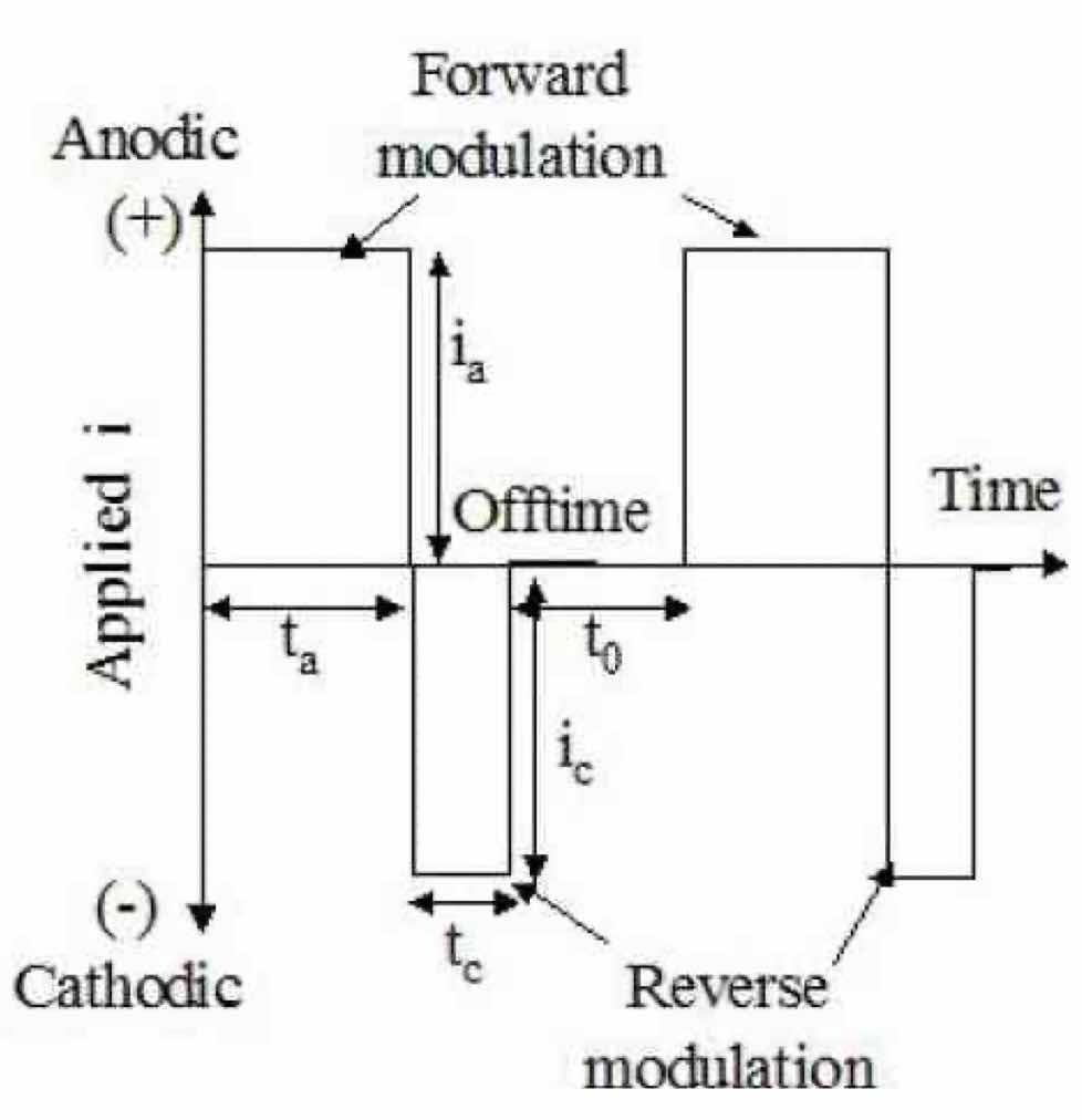 Figure 1—Generic pulse/pulse reverse waveform.Advanced materials form an oxide film that is self-healing and reforms in the presence of oxygen or even water. Since this passive film has low electrical conductivity and prevents the workpiece from a direct contact with the electrolyte, normal anodic dissolution cannot proceed without breakdown of the film. For conventional electrochemical polishing and non-steady state processing, high cell voltages and/or highly toxic acids such as HF are required to breakdown the oxide passive layer. Partial breakdown of the oxide film often occurs which causes pits on the surface. The proposed pulse/pulse reverse polishing process addresses this pitting problem by reducing the passive film during the reverse period. By properly adjusting the process parameters, we can selectively consume the nascent oxygen gas or the oxide film on the workpiece by the following reactions:
1⁄2O2 + 2H+ _ 2e → H2O (2)
M(Ox) + 2xH+ + 2xe → M + xH2O (3)
Therefore, the pulse/pulse reverse process can reduce/eliminate the oxide film rehealing and eliminate the pits associated with partial oxide film breakdown.
Mass transport effects
The theory of mass transport during pulsed electrolysis has been discussed previously.14,15,16 In steady-state electrolysis (i.e., constant current processes), the diffusion layer thickness, δ, is a time-invariant quantity for a given cell geometry and the solution hydrodynamic condition that develops within it. In pulsed electrolysis, δ begins to establish itself as soon as the electric field is applied. Therefore, the diffusion layer thickness is zero at the beginning of the pulse and gradually increases to its steady state value, which is what happens during a direct current process. In pulsed electrolysis, however, the current can be interrupted before δ is fully established. By selecting the appropriate subsequent off-time, this allows the dissolved ions to diffuse away from the electrode surface and allow the surface concentration to drift back to its original value before the next current interruption. Therefore, the concentration of reacting species in the vicinity of the electrode pulsates with the frequency of the modulation. The corresponding diffusion limiting current density, which is a measure of the removal rate, would be equal to an infinite value at time zero and decrease to a steady state value equivalent to the DC limiting current density.
The scientific basis for the previous paragraph is provided by work published by Ibl and colleagues,17,18,19 where a “duplex diffusion layer,” consisting of an inner pulsating layer and an outer stationary layer was developed. Modeling work by Landolt has also suggested the existence of a pulsating diffusion layer.20 Since the thickness of the pulsating diffusion layer is determined by the waveform parameters, we call this layer the “electrodynamic diffusion layer” (Fig. 2).21 By assuming a linear concentration gradient across the pulsating diffusion layer and conducting a mass balance, Ibl derived the pulsating diffusion layer thickness (δp) as:18
δp = (2Dton)1⁄2 (4)
where D is the diffusion coefficient and ton is the pulse length. When the pulse on-time is equal to the transition time (τ), the concentration of reacting species at the interface drops to zero precisely at the end of the pulse. An expression for τ is provided in the following equation:
τ = [(nF)2Cb2D]/2ip2 (5)
More exact solutions are given by integrating Fick’s diffusion equation:
δp = 2[(Dton)/π)1⁄2 (6)
τ = π[(nF)2Cb2D]/4ip2 (7)
More recently, Yin,22 using a similar approach to Ibl’s, derived the same equation for the pulsating diffusion layer for “pulse-withreverse” electrochemical processes. The ratio between the limiting current density realized in the pulse/pulse reverse process, ip, versus that in steady state, ilim, is:
ip/ilim = [δp/δ (1 - γa) + γa]-1 (8)
Since δp must be smaller than δ, higher instantaneous limiting current densities can be achieved in pulsed processes. The extent of this increase is based on the δp/δ ratio, which is directly influenced by the anodic pulse on-time. A higher limiting current density relates directly to a higher instantaneous metal removal rate. Therefore, the overall removal rate of a pulsed process can rival that of a DC process despite a duty cycle that is less than 100%, while enjoying enhanced process performance.
Another key consideration when trying to design a waveform for a particular finishing environment is the current distribution that will develop. There are two important aspects that must be taken into account. First, is the current distribution a function of primary (geometrical), secondary (kinetic) or tertiary (mass transport) considerations? Second, what is the relationship between the pulsating boundary layer thickness and the surface profile height?
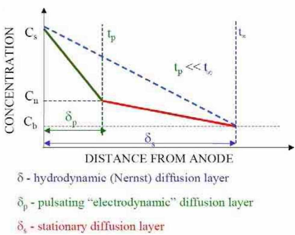 Figure 2—Schematic representation of the duplex diffusion layer.First, the current distribution developed in constant current processes is controlled by primary effects. Through the application of pulsed electric fields, the pulse/pulse reverse process supplements the primary effects with both secondary and tertiary effects. The addition of these effects tends to make the current distribution more uniform, as compared to primary current distribution alone. Therefore, the current distribution in the pulse/pulse reverse process can be substantially different than that achieved in conventional constant current processes. By understanding the influence of the pulse waveform parameters on current distribution, parameters can be selected to enhance either localized current distribution (for surface leveling or edge deburring) or uniform current distribution (for surface polishing).
If the waveform is selected such that the pulse on-time is much longer than the transition time, tertiary effects play a dominant role in the current distribution. For this case, additional criteria that influence current distribution are the concepts of macroprofile and microprofile. In a macroprofile (Fig. 3, left), the roughness of the surface is large compared with the thickness of the diffusion layer, and the diffusion layer tends to follow the surface contour. Under mass transport or diffusion control, a macroprofile results in a uniform current distribution and conformal dissolution. In a microprofile (Fig. 3, right), the roughness of the surface is small compared with the thickness of the diffusion layer. Under mass transport or diffusion control, a microprofile results in a localized current distribution and non-uniform dissolution. Note that in the absence of mass transport control, the primary and/or secondary current distribution effects control the process.
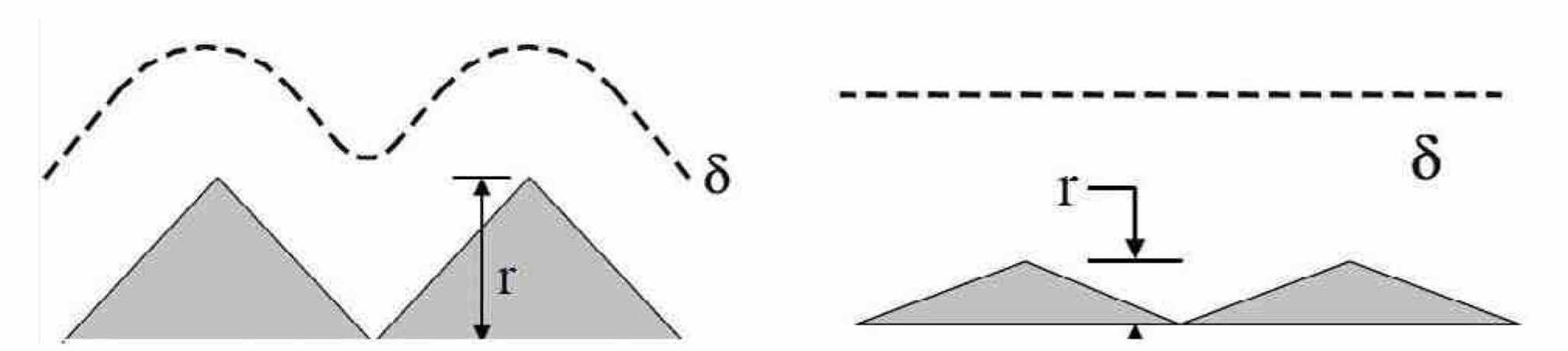 Figure 3—Left: macroprofile (δ ~ r); right: microprofile (δ > r).
Waveform sequencing
Our experience has also shown the need for waveform sequencing (Fig. 4) when polishing surfaces to a very low Ra. Depending on the flow rate of electrolyte past the surface, a macroprofile may initially exist, and a specific waveform is chosen to polish this surface. As the surface is polished and becomes much smoother, the macroprofile may transition to a microprofile. In order for further polishing (lower Ra) to be achieved, the waveform must be changed. An advantage of the pulse/pulse reverse process is that these distinct waveforms may be preprogrammed into the rectifier, so that process control is simplified. We have used this approach to electropolish stainless steel valves to an Ra of 0.12 μm for a customer application.
Experimental Procedure
Sample preparation
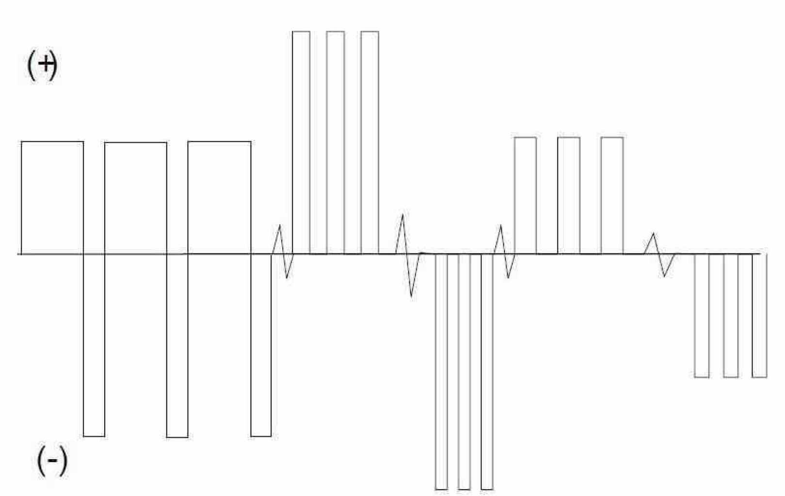 Figure 4—Generic waveform sequencing, used to electropolish materials to a very low Ra.Niobium foil, 99.9% pure (Goodfellow Corporation, Oakdale, PA.) was purchased (Fig. 5) and cut into same size coupons for the electropolishing studies. Final coupon sizes had the following dimensions: 25.4 mm × 25.4 mm × 3 mm (Fig. 6). Since a high precision cut was needed, wire electrical discharge machining (WEDM) was employed. As WEDM is an electrothermal process, there was formation of an oxide layer on the sample being cut. As can be observed in Fig. 6, the niobium coupon after WEDM was darker as compared to the stock material shown in Fig. 5. Therefore, mechanical polishing was employed in order to remove the oxide layers and obtain a standardized surface finish before the electropolishing experiments.
Electrochemical cell
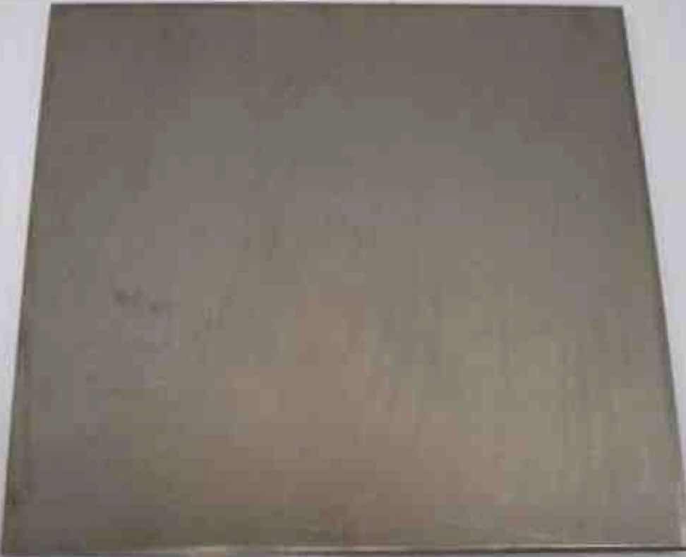 Figure 5—15 cm × 15 cm × 0.3 cm Nb foil, 99.9% pure.Figure 7 shows the photograph (left) and an AutoCAD drawing (right) of a low flow channel cell that accommodates the 25.4 mm × 25.4 mm × 3 mm niobium coupons. This cell allowed the study of electropolishing niobium at different cathode-to-anode distances, as well as different electrolyte velocities. The flexibility inherent within this cell design enabled an investigation of the effect of primary current distribution in conjunction with the pulse/ pulse reverse process for electropolishing niobium.
The 25.4 mm × 25.4 mm × 3 mm coupons were mechanically polished using 60-grit or 180-grit silicon carbide (SiC) grinding paper, giving an initial Ra of approximately 1.53 μm or 0.56 μm, respectively. The niobium coupons were cleaned ultrasonically using a Branson ultrasonic cleaner (Model 3510) in 5% NaOH and DI water. Only an area of 12.7 mm × 12.7 mm of the niobium coupon was used for DC polarization studies and electropolishing experiments. The rest of the area was masked with plating tape to avoid edge effects.
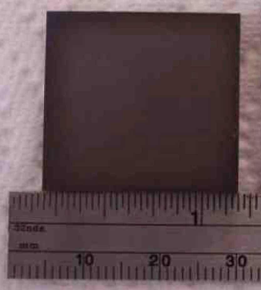 Figure 6—25 mm × 25 mm × 3 mm Nb coupon after WEDM.
Electrolyte selection
Development of the pulse/pulse reverse process typically begins with a polarization curve study, which is a plot of the anode voltage, Ea, as a function of anodic current density, ia, and provides information on active and passive regions of materials in different electrolytes.23 Generic polarization curves, shown in Fig. 8, illustrate the anodic behavior of a metal in various electrolytes. Curve 1 shows the behavior of a metal in an active electrolyte (such as NaCl), and Curve 2 shows the behavior of a metal in a passive electrolyte (such as Na2SO4). Before the electric field is applied, the metal anode immersed in the electrolyte has a steady-state voltage (Ess). When the power is applied, the electrode voltage will shift in the positive direction from Ess to Eab (the breakdown voltage). Above Eab, the current density rises abruptly due to the dissolution reactions occurring on the anode (region AB). The dissolution rate of the anode metal stops increasing when a limiting current density ilim is reached (BC region), where the metal atoms form metal ions and compounds with the activating anions and pass into the electrolyte. The limiting current density ilim and the ratio of ∆I to ∆E (the slope of AB on the polarization curve) can be defined as the metal dissolution rate and current efficiency in the electrolyte, respectively.
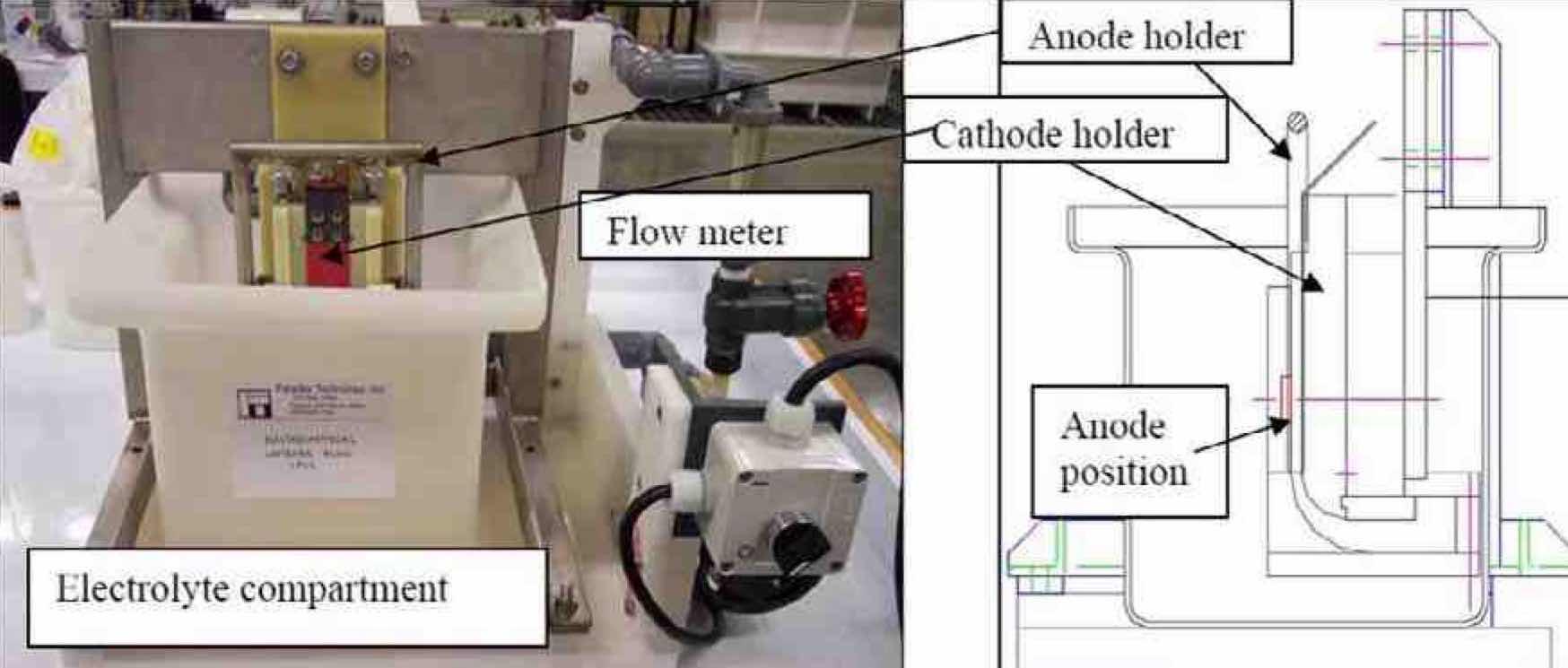 Figure 7—Photograph (left) and side view AutoCAD drawing (right) of the low flow channel cell used to electropolish 25.4 mm × 25.4 mm × 3 mm Nb coupons.
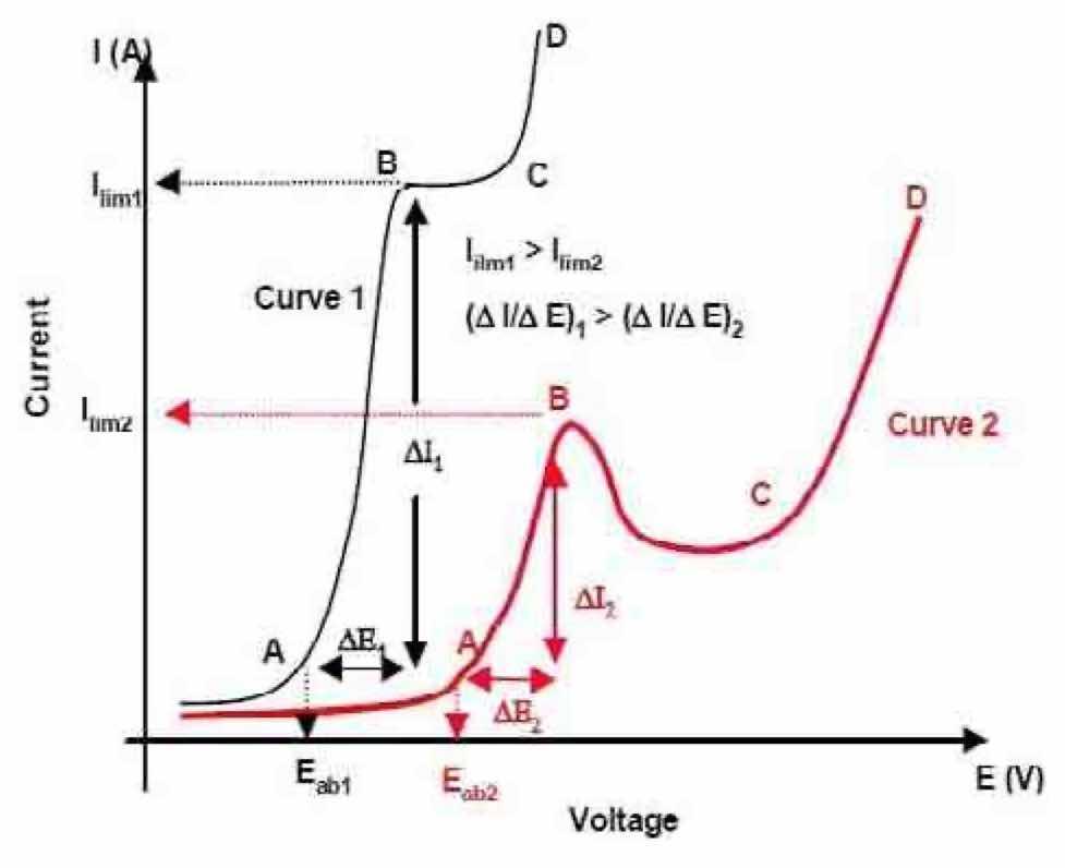 Figure 8—Typical polarization curves for metal in different electrolytes.DC polarization studies were carried out in order to select an electrolyte that would enable the process for electropolishing niobium coupons. The two-electrode DC polarization studies were performed on 25.4 mm × 25.4 mm × 3 mm niobium coupons to study the electrochemical activity (e.g., total current density) of niobium in different electrolyte type and concentrations. A platinum-coated niobium mesh was used as the cathode. All polarization curve experiments were performed at room temperature (~20°C). A TecNu power supply was used for this study (Model SPR-300/100/48-3). The cell voltage was raised by increments of five volts per minute. Total current densities were read from the oscilloscope trace recorded on a FLUKE 196C Scopemeter color system.
Results and Discussion
Polarization curve study
 Figure 9—Two-electrode polarization curves of Nb in different electrolytes.Figure 9 summarizes the electrochemical activity of niobium substrates in different electrolytes, low and high concentrations of sodium chloride (NaCl), sulfuric acid (H2SO4), sodium bromide (NaBr), sodium fluoride (NaF) and phosphoric acid (H3PO4). In all cases, no breakdown of the niobium was observed. Any current measured is assumed to be associated with water oxidation (2H2O → O2 + 2H+ + 2e-) and niobium anodization. The highest and lowest total current density observed for voltages up to 70 V was in the H2SO4and NaF electrolytes, respectively.
This data demonstrates the tenacity of the niobium oxide film. DC polarization studies were unable to shed any light on the conditions that would be required to break down the oxide film without the use of hydrofluoric acid. Therefore, based on our prior experience in surface finishing of passive materials, we chose to develop electrochemical waveforms to electropolish niobium. Historically, we have combined the waveforms with process parameters such as cell geometry and uniform hydrodynamic conditions for successful metal removal of passive metal and alloys.13,24 An advantage of electrolyte flow is the removal of undesired byproducts from the surface of the substrate being electropolished, such as niobium ions, heat and bubbles (resulting mainly due to oxygen and hydrogen generation from water electrolysis).
 Figure 10—Representative Nb coupons after electropolishing experiments at ambient temperature (~20°C) in H2SO4 electrolytes using their respective pulse/pulse reverse waveforms listed in Table 1.
Electropolishing of niobium
In the initial experiments, the constant parameters were electrolyte velocity = 0.4 m/sec, run time = 10 min, forward (Vf) and reverse voltage (Vr), anode-to-cathode distance = 5 mm, and ambient temperature (~20°C). Since the electrochemical cell did not have temperature control built in, the electrolyte temperature rose from an initial value of 20°C to around 27°C by the end of every experiment. A design of experiments set was performed using MINITAB. Two different frequencies were used at two different forward duty cycles (Df) (Table 1).
Table 1: Design of experiments using pulse/pulse reverse waveforms to electropolish Nb in a H2SO4electrolyte for 10 min and an anode-cathode distance of 5 mm
| Run No. | Waveform No. | Frequency | Forward (Anodic) Duty Cycle % | Vf | Vr |
| 1 | PRC1 | Low | High | Low | Constant |
| 2 | PRC2 | High | Low | Low | Constant |
| 3 | PRC3 | Low | Low | Low | Constant |
| 4 | PRC4 | High | High | Low | Constant |
Figure 10 shows representative niobium coupons after electropolishing experiments were attempted in a H2SO4 electrolyte using the pulse/pulse reverse waveforms in Table 1. Run #1 (Fig. 10-left) showed no evidence of etching. The different colors observed represent niobium oxide layers formed on the substrate. Run #2 (Fig. 10-center) showed some degree of etching, which suggested that niobium substrates could be uniformly electrochemically etched in an electrolyte free of HF. Run #4 (Fig. 10-right) also showed some degree of etching, but much lower as compared to Run #2.
 Figure 11—Nb coupon of Run #5 after electrochemical polishing at 2.7 μm/min in a H2SO4 electrolyte.Based on these preliminary results, the pulse/pulse reverse waveform used for Run #2 was further explored. Specifically, Run #5 used the same waveform parameters as Run #2, but the coupon was electropolished for 37 min instead of 10 min. The resulting niobium coupon surface is shown in Fig. 11. A thickness of 100 μm of niobium was successfully removed uniformly from the coupon at an average removal rate of 2.7 μm/min over an area of approximately 161 mm2.
Having achieved uniform removal of niobium in an HF-free electrolyte, the next step was to optimize the electropolishing process to achieve surface roughness similar or better to the ones obtained by state-of-the-art electropolishing techniques (e.g., around 0.1 to 0.2 μm). The following process and cell parameters were studied:
- Effect of applied peak voltage
- Effect of polishing time
- Effect of anode-to-cathode distance
- Effect of electrolyte flow velocity
Effect of peak voltage on niobium electropolishing
The effect of raising Vf in PRC2 (Vf = low potential) on niobium electropolishing performance was studied. Two higher forward voltages were explored, PRC5 (Vf = intermediate potential) and PRC6 (Vf = high potential). In both cases, the other pulse/pulse reverse process parameters, frequency, Df and Vr were kept the same as for waveform PRC2.
 Figure 12—Nb coupons after electropolishing in a H2SO4 electrolyte at room temperature (~20°C) at varying Vf: (a) Run #5 (PRC2); (b) Run #6 (PRC5) and (c) Run #7 (PRC6).
Figure 12 shows niobium coupons of Runs #5 (PRC2), #6 (PRC5) and #7 (PRC6), after electropolishing in a H2SO4 electrolyte, varying Vf. Figure 13 summarizes the effect of peak voltage on niobium surface finish. The roughest surface finish was obtained using PRC2. When Vf was increased in PRC5, the surface finish Ra of niobium dropped from 1.38 μm to 0.29 μm. When PRC6 was used, the niobium surface finish started getting rougher again and surface discoloration was observed. Therefore, for future experiments during this work, we used waveform PRC5.
Effect of electropolishing time on niobium surface roughness, Ra
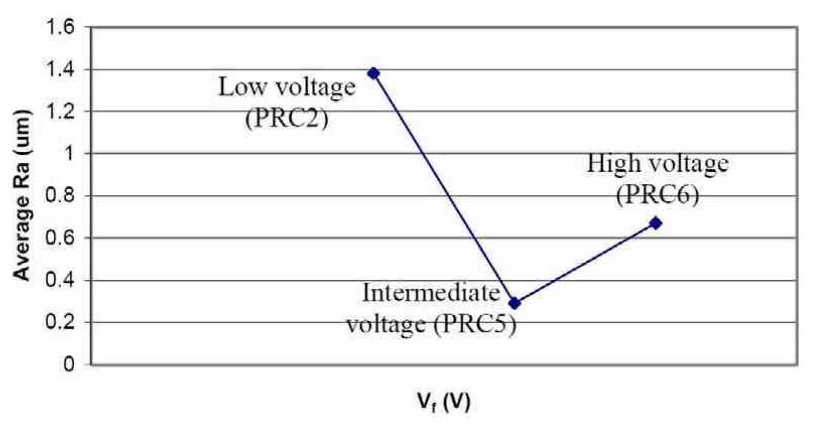 Figure 13—Effect of Vf on the average surface roughness of Nb after electropolishing in H2SO4 electrolytes at ambient temperature (~20°C); Run #5 (PRC2), Run #6 (PRC5) and Run #7 (PRC6).Once a set of process parameters for polishing niobium in H2SO4 had been determined, the next phase of study was aimed at minimizing unnecessary polishing time. The optimum waveform (to date) developed previously (PRC5) was applied to a niobium coupon in 10-min steps. After each 10-min step, the coupon was removed from the cell, rinsed with DI water and dried with compressed air, and the Ra was measured. The coupon was then returned to the electrochemical cell for a further 10 min of electropolishing.
Figure 14 shows the effect of electropolishing time on the average surface roughness of a niobium coupon using waveform PRC5. The surface finish decreased slowly with time until 30 min of polishing had been applied, and then there was a more rapid decrease in Ra down to 0.2 μm between 30 and 50 min. After 50 min, further decreases in Ra were not observed. This result suggests the need for waveform sequencing, as briefly discussed in the Introduction section, to further decrease the niobium surface roughness.
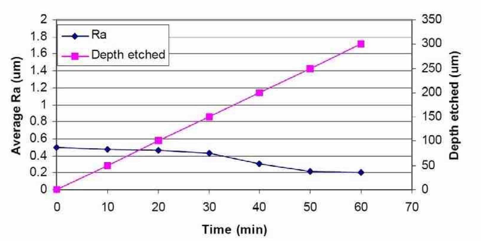 Figure 14—Effect of time on the average surface roughness of Nb after electropolishing in a H2SO4 electrolyte at ambient temperature (~20°C), using waveform PRC5, and Rao = 0.56 μm (Run #8).During electropolishing, the material removal rate was constant, at approximately 5.0 μm/min, about ten times faster than conventional electropolishing techniques that use HF.
The effect of the niobium initial surface roughness, Rao on the final surface roughness, Raf was also studied by performing electropolishing time studies at different Rao values. Figure 15 compares the effect of time on the average surface roughness of a niobium coupon after electropolishing in a H2SO4 electrolyte for Rao = 0.56 μm (Run #8) and Rao = 1.53 μm (Run #9). For the higher initial surface roughness, there was a significant decrease in Ra after 10 min, from 1.53 μm to ~0.85 μm. Thereafter, Ra was decreased further by increasing the electropolishing time up to 60 min down to an Raf value of 0.33 μm. Further decreases in surface finish did not occur after 50 min, again suggesting the need for waveform sequencing to obtain a lower Ra.
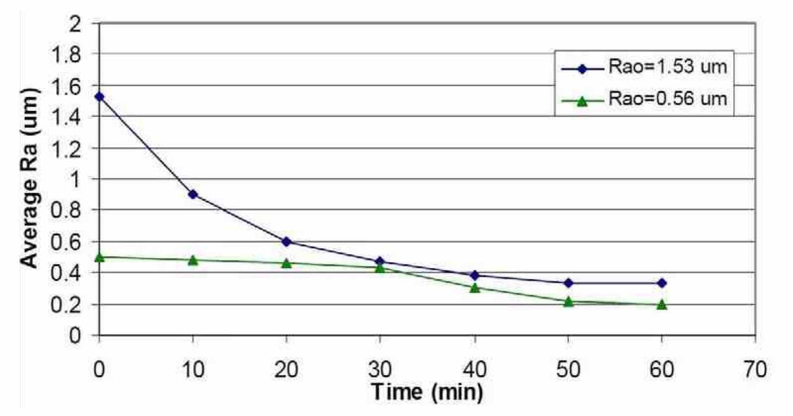 Figure 15—Effect of time on the average surface roughness of Nb after electropolishing in H2SO4 electrolytes at room temperature (~20°C) using waveform PRC5 and different Rao values.
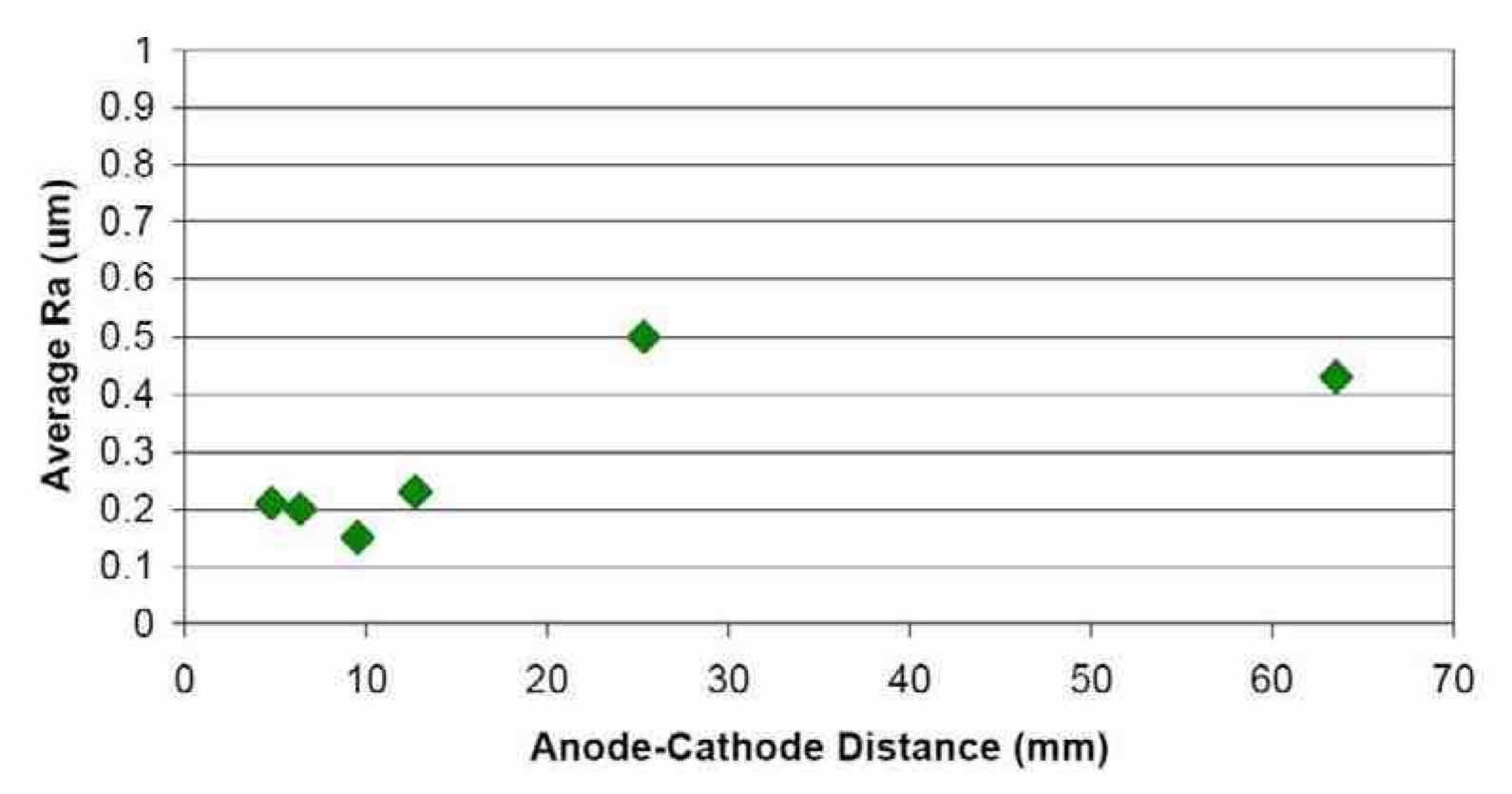 Figure 16—Effect of anode-to-cathode distance on the average surface roughness of Nb after electropolishing in a H2SO4 electrolyte at ambient temperature (~20°C), using waveform PRC5. Experiments correspond to Runs #10 through #15 in order.
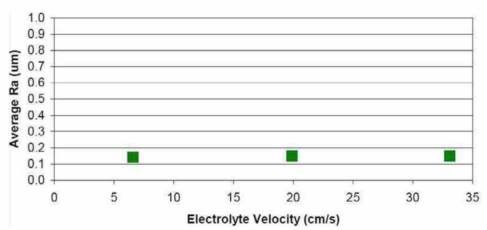 Figure 17—Effect of electrolyte velocity on the average surface roughness of Nb after electropolishing in a H2SO4 electrolyte at ambient temperature (~20°C), using waveform PRC5 and an anode-to-cathode distance of 10 mm.
Effect of varying cell parameters on the Ra of electropolished niobium
The effects of anode-cathode distance as well as electrolyte velocity on the surface roughness of electropolished niobium were studied. The effect of anode-cathode distance and electrolyte velocity on niobium surface finish was studied using waveform PRC5 at ambient temperature (~20°C). Each experiment ran for 40 min in a H2SO4 electrolyte.
Effect of anode-to-cathode distance on Ra: The results of the anode-to-cathode distance study are summarized in Fig. 16. For anode-to-cathode distances up to 10 mm, Ra decreased to a minimum value of 0.15 μm. At anode-to-cathode distances greater than 10 mm, Ra increased with anode-to-cathode distance, becoming almost flat at distances larger than 25 mm. After the anode-to-cathode distance study, all subsequent experiments were performed with the cell geometry at which an Ra value of 0.15 μm was obtained (an anode-to-cathode distance of 10 mm).
Effect of electrolyte velocity on Ra: The effect of electrolyte velocity was another important variable that was studied to understand its effect on niobium electropolishing. In these experiments, the anode-to-cathode distance used was 10 mm. The results are summarized in Fig. 17. Three different electrolyte velocities were explored, 33.1 cm/sec (Run #16), 19.9 cm/sec (Run #17) and 6.6 cm/sec (Run #18). The final Ra values were 0.14, 0.15 and 0.15 μm, respectively. The photographs of bright and smooth polished niobium substrates corresponding to each run are shown in Fig. 18. There did not appear to be a significant effect of electrolyte velocity when electropolishing niobium in this cell configuration. However, the results of an experiment with an electrolyte velocity of 0 cm/sec (Run #19), suggested that there must be some degree of agitation in order to achieve uniform, smooth polishing of the niobium surface.
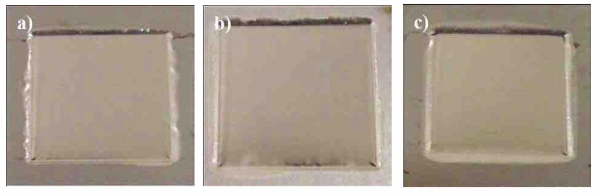 Figure 18—Photographs of Nb coupons after electropolishing in H2SO4 electrolytes at room temperature (~20°C), using waveform PRC5, an anode-to-cathode distance of 10 mm and varying the electrolyte velocity: (a) 6.6 cm/sec, (b) 19.9 cm/sec and (c) 33.1 cm/sec.
Characterization of electropolished niobium substrates
Effect of profilometer scan length on Ra: The effect of the profilometer scan length on the average surface roughness, Ra, was studied. Figure 19 shows the effect of scan range on the Ra value of niobium after electropolishing in H2SO4electrolytes using waveform PRC5 at different electrolyte velocities. Two different scan lengths, 1.25 mm and 4 mm, were used on the same area of the electropolished niobium coupons. The effect of scan range on Ra was almost identical for the three different electrolyte velocities. Ra increased slightly from around 0.1 μm to 0.15 μm by increasing the scan length from 1.25 mm to 4.0 mm. This data suggests that the macroscale surface roughness is slightly higher than the microscale roughness.
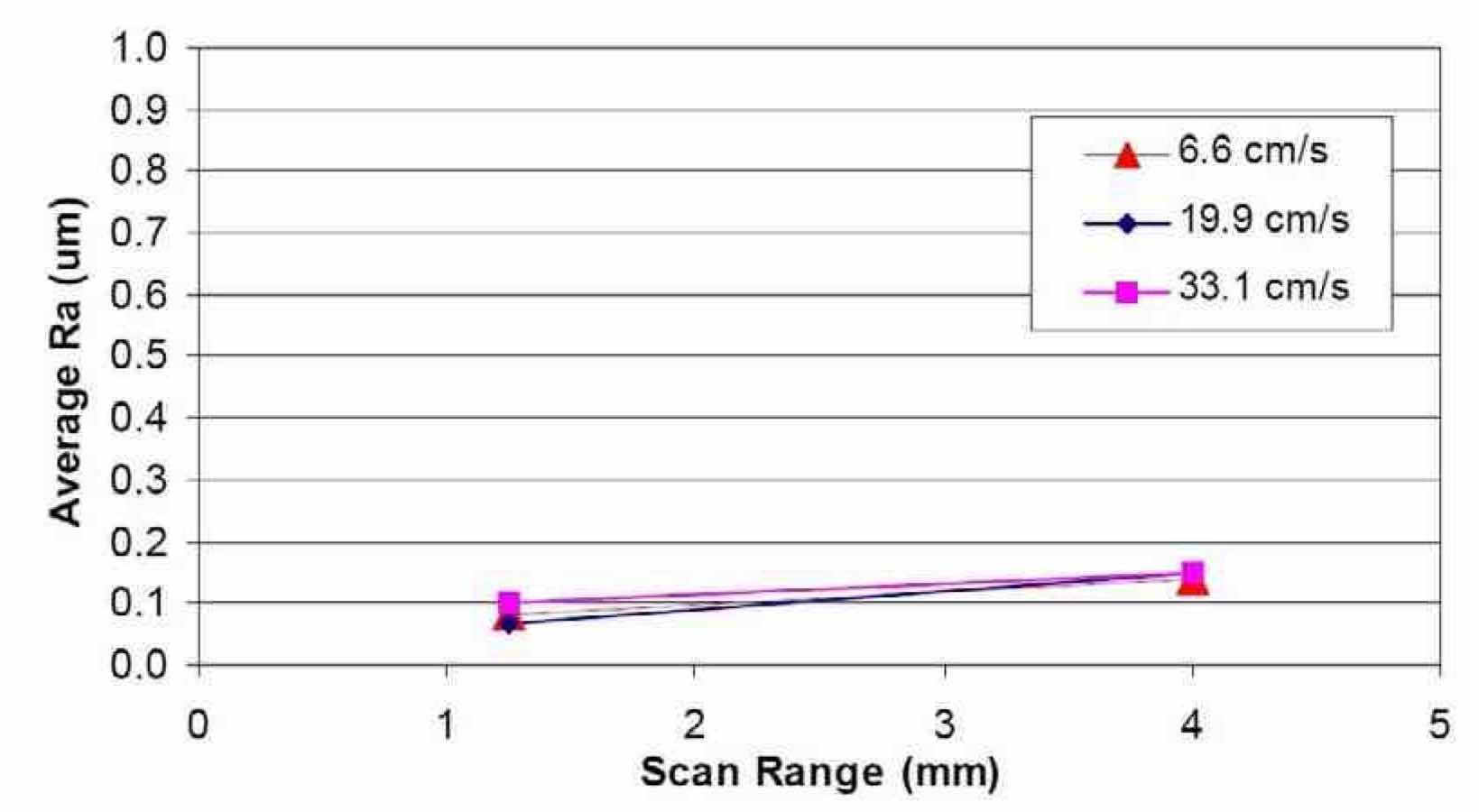 Figure 19—Effect of scan range on the average surface roughness of Nb after electropolishing in H2SO4 electrolytes, using waveform PRC5 and different electrolyte velocities.
Scanning electron microscopy evaluation: Figure 20 shows an SEM micrograph of the surface morphology of a niobium substrate electropolished using a H2SO4 electrolyte, waveform PRC5 at a velocity of 6.6 cm/sec and anode-to-cathode distance of 10 mm. The image confirms that a smooth surface of niobium can be obtained, not only at a macroscale, but also at a microscale finish using the pulse/pulse reverse process in an electrolyte free of HF.
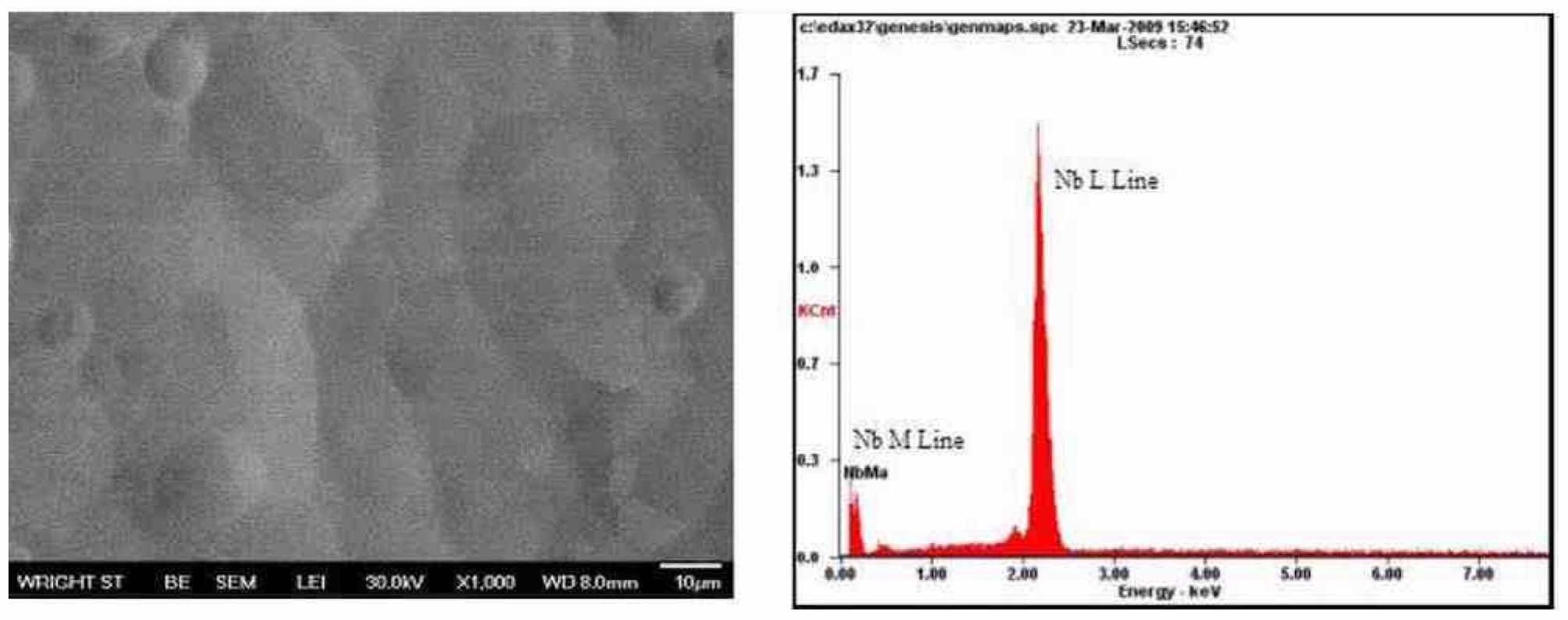 Figure 20—SEM micrograph (left) and EDS of a Nb substrate after electropolishing in H2SO4 electrolytes at room temperature (~20°C), using waveform PRC5, an anode-to-cathode distance of 10 mm and an electrolyte velocity of 6.6 cm/sec.
Energy Dispersive Spectroscopy (EDS) was used to analyze the surface of electropolished niobium coupons. Figure 20 (right) shows an EDS spectrum of the elements detected on the surface of the analyzed area on the niobium substrate. The spectrum was mainly dominated by the presence of niobium. Dr. Allen G. Jackson, Program Manager of the Department of Mechanical & Materials Engineering at Wright State University, who performed the SEM and EDS analysis, believes that even though oxygen is present in very small amounts (he estimates about 0.5 wt%), its peak is too small to be statistically significant. In such a case, the small amounts of oxygen would correspond to a very thin layer of Nb O (about 5 nm thick) that forms naturally on niobium. The 25 elements and their respective weight percentages are listed in Table 2. There was no evidence of impurities present on the niobium surface using EDS analysis.
Table 2: List of elements and wt% detected using EDS on Nb substrates after electropolishing in H2SO4 electrolytes at room temperature (~20°C), using waveform PRC5, an anode-to-cathode distance of 10 mm and an electrolyte velocity of 6.6 cm/sec
| Element | Weight% | Atomic% |
| Niobium (Nb) | 99.5 | 97.2 |
| Oxygen (O) | 0.5 | 2.8 |
Summary of results
Table 3 compares the pulse/pulse reverse electropolishing process with chemical polishing and conventional electropolishing, state-of-the-art techniques employed to polish superconducting radio frequency accelerators made of niobium. Unlike chemical and conventional electropolishing, the pulse/pulse reverse process does not use hydrofluoric acid, achieving electropolishing rates up to five to ten times faster, respectively. Surface roughness values average of about one order of magnitude lower than obtained by chemical polishing.
Table 3: Summary table comparing chemical polishing conventional electropolishing and pulse/pulse reverse electropolishing
| Chemical polishing | Conventional electrochemical polishing | Pulse/pulse reverse electropolishing | |
| Electrolyte | HF/HNO3/H3PO4 (1:1:3) | HF (10%): H2SO4 (90%) | H2SO4 |
| Hydrofluoric acid | Yes | Yes | No |
| Etch rate μm/min | 1.0 | 0.5 | 5.0 |
| Ra μm | 1.0 | 0.1 | 0.1 |
| Temperature °C | 15 (Chilled) | 30-35 (Chilled) | 20 |
Conclusions
The overall objective of this work was to demonstrate the technical and economic feasibility of the pulse/pulse reverse process for polishing niobium for superconducting radio frequency cavities in an environmentally benign electrolyte. Results indicated that the pulse/pulse reverse process could (a) uniformly electropolish niobium to a microscale finish (0.1 μm) in a hydrofluoric acid-free electrolyte and (b) increase electropolishing rates about 10 times faster than state-of-the-art techniques that use hydrofluoric acid. In addition, SEM/EDS analysis showed that electropolished niobium surfaces free from contamination were obtained.
The results/attributes just mentioned, make the pulse/pulse reverse HF-free electropolishing process an ideal polishing technique not only for niobium cavities, but also for surgical devices and metallic implants made of niobium, titanium, titanium-nickel and stainless steel alloys. The process is anticipated to be cost effective compared to conventional polishing methods due to the robust control mechanisms and minimal associated waste.
Acknowledgement: This material is based upon work supported by the Department of Energy under Award Number DE-FG02-08ER85053.
Disclaimer: This report was prepared as an account of work sponsored by an agency of the United States Government. Neither the United States Government nor any agency thereof, nor any of their employees, makes any warranty, express or implied, or assumes any legal liability or responsibility for the accuracy, completeness, or usefulness of any information, apparatus, product, or process disclosed, or represents that its use would not infringe privately owned rights. Reference herein to any specific commercial product, process, or service by trade name, trademark, manufacturer, or otherwise does not necessarily constitute or imply its endorsement, recommendation, or favoring by the United States Government or any agency thereof. The views and opinions of authors expressed herein do not necessarily state or reflect those of the United States Government or any agency thereof.
References
- Saito, Proceedings of the 2003 Particle Accelerator Conference, p. 462 (2003); http://accelconf.web.cern.ch/ accelconf/p03/PAPERS/ROAA002.pdf (last accessed 09/14/ 09).
- “Argonne-Fermilab BCP System Coming Together,” ILC Newsline (4 January 2007); http://www.linearcollider.org/ newsline/archive/2007/20070104_feature1.pdf (last accessed 09/14/09).
- T. Wu, et al., Applied Surface Science, 253 (6), 3041 (2007).
- Lilje, et al., Nuclear Instruments and Methods in Physics Research A, 524 (1-3), 1 (2004).
- Mickova, et al., Croatica Chemica Acta, 79 (4), 527 (2006); http://hrcak.srce.hr/index.php?show=clanak&id_clanak_ jezik=8911; link to full text (last accessed 09/14/09).
- D. Zardiackas, M. J. Kraay & H. L. Freese, Titanium, Niobium, Zirconium, and Tantalum for Medical and Surgical Applications, ASTM International, Materials Park, OH, 2006; p. 268.
- Jiin-huey Chern, J. Chien-ping & L. Chih-min, U.S. Patent 6,752,882 (2004).
- Personal communication, Prof. Lyle Zardiackas, April 8th, 2009.
- Eliaz & O. Nissan, J. Biomedical Materials Research Part A, 83A (2), 546 (2007).
- W. Dini, Electrodeposition-The Materials Science of Coatings and Substrates, Noyes Publications, Park Ridge, NJ, 1993; Chapter 7, p. 56.
- J-C. Puippe & F. Leaman, Theory and Practice of Pulse Plating, NASF, Washington, DC, 1986.
- J. Sun, et al., Plating & Surface Finishing, 89 (5), 94 (2002).
- Lozano-Morales, et al., J. Appl. Surf. Finish., 2 (3), 192 (2007).
- Y. Cheh, J. Electrochem. Soc., 118, 551 (1971).
- Y. Cheh, J. Electrochem. Soc., 118, 1132 (1971).
- Viswanathan, M.A. Farrell-Epstein & H.Y. Cheh, J. Electrochem. Soc., 125, 1772 (1978).
- Ibl, J. C. Puippe & H. Angerer, Surface Technology, 6 (4), 287 (1978).
- Ibl, Surface Technology, 10 (2), 81 (1980).
- Ibl, Proc. 2nd International Pulse Plating Symposium, NASF, Washington, DC, 1981.
- Landolt, in Theory and Practice of Pulse Plating, J-C. Puippe & F. Leaman, Eds., NASF, Washington, DC, 1986.
- J. Taylor, et al., Proc. AESF SUR/FIN 2001, NASF, Washington, DC, 2001; p. 504; also in Plating & Surface Finishing, 89 (5), 88 (2002).
- K-M. Yin, Surface and Coatings Technology, 88 (1-3), 162 (1996).
- Rumyantsev & A. Davydov, Electrochemical Machining of Metals, MIR Publishers, Moscow, 1989.
- J. Sun, E. J. Taylor & R. Srinivasan, J. Materials Processing Technology, 108 (3), 356 (2001).
About the Authors (as of 2009)
Dr. Alonso Lozano-Morales is a Project Engineer at Faraday Technology, Inc. He received his B.S. from Universidad de Sonora, Mexico and his Ph.D. degree from Louisiana State University, Baton Rouge, LA. All the above degrees are from the Department of Chemical Engineering. Currently, he is leading Faraday Technology’s edge and surface finishing process technology development, as well as industrial coatings.
Dr. Maria E. Inman is the Research Manager at Faraday Technology Inc. She holds a B.E. in Metallurgical and Materials Engineering and a Ph.D. in Materials Engineering from the University of Auckland, New Zealand. Prior to joining Faraday Technology, she completed a two-year term as a post-doctoral research associate at the Center for Electrochemical Science and Engineering at the University of Virginia.
Dr. E. Jennings Taylor is the CEO and IP Director at Faraday Technology, Inc., Clayton, OH. He founded the company to develop and commercialize innovative electrochemical technology using sophisticated charge-modulated electric fields. The company’s intellectual property has been successfully transferred both to government agencies and large manufacturers in the form of process engineering technology and products. He holds a B.A. in chemistry from Wittenberg University, an M.A. in technology strategy and policy from Boston University, and M.S. and Ph.D. degrees in materials science from the University of Virginia. He has published more than 70 technical papers and articles and holds many patents. He serves on the AESF Pulsed Electrodeposition Processes Committee and is Chairman of the Research Board.