


Copper metallization of interconnects is an important process in the manufacture of printed circuit boards (PCBs).
 Stephen Snyder, Holly Garich, Burhanuddin Kagajwala, and E. Jennings Taylor Many current PCB designs rely on the use of multilayer interconnects (or z-interconnects) to facilitate higher numbers of devices on a single chip and, thus, smaller electronic devices to meet consumer needs. While the use of z-interconnects achieves these needs, any voids and non-uniformities of the copper in the z-interconnects may result in deposit fatigue and deposit cracking, which may result in short-circuiting and product failure or poor PCB performance.1,2,3
Electroplating is the standard fabrication technique for the metallization of z-interconnects.4 However, technological advances in circuit boards are, in general, limited by the plating process in PCB manufacturing facilities.1 Uneven localized current distribution (which causes the commonly encountered edge effects) results in thin inner-layer plating (i.e., low throwing power), “dog-boning” on the feature knees, or voiding in a z-interconnect fill process. This causes manufacturers to resort to creative techniques to improve z-interconnect uniformity, such as use of complex additive chemistries, use of low current densities, surface overplate to achieve thicker deposits in the barrel, changing panel orientation during the plating process, use of pulse reverse processes, and/or the manipulation of plating tank geometry. Many of these methods are costly to the manufacturing bottom line, as they increase materials, operating and maintenance costs, or decrease throughput. Optimization of the plating cell geometry, to ensure uniform boundary layer thickness, is an imperative part of improving manufacturing costs and production of high reliability panels.
The patented electrochemical cell**,5,6,7 was designed and engineered to deliver uniform boundary layer thickness across flat substrates, including PCBs, which results in higher levels of copper thickness uniformity when compared to other plating cell geometries.8 In general, we use pulse reverse electric fields in the absence of complex plating chemistries in the cell. However, the cell geometry is applicable to any process, including direct current (DC) processes and/or processes utilizing complex plating chemistries. Furthermore, while the current paper discusses the technology as it pertains to copper metallization for PCBs, the cell geometry is relevant to any electrochemical process (electrodeposition, electropolishing or electrochemical machining) and has been demonstrated for many industrial applications.
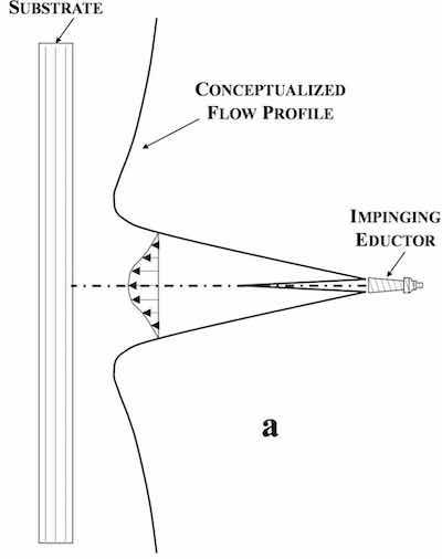 Figure 1 - Schematic representation of impinging eductor configuration and resulting velocity profile.The boundary layer thickness and consequent plating uniformity are governed by cell geometry and electrolyte agitation mechanisms. Traditionally, air sparging was the standard agitation mechanism employed in plating baths, but eductor agitation has become more commonplace in industrial practice. Air sparging has a number of associated disadvantages, including lodging of air bubbles in the PCB feature (and consequent plating voids), low solution agitation, and non-uniform solution flow that results in non-uniform boundary conditions. Eductor agitation has, in general, replaced air sparging as the agitation mechanism of choice. This method amplifies the solution flow velocity output of the pump, and, in theory, creates a thinner boundary layer condition when compared to pump velocity alone.
While the benefits of eductor agitation are obvious, poorly utilized eductor geometry may limit the usefulness of the technology. Commonly utilized eductor configurations are shown schematically in Fig. 1 (impinging eductor orientation) and Fig. 2 (glancing eductor orientation) with their resulting velocity profiles.9,10,11 Impinging eductors are oriented either perpendicular to or parallel with the substrate surface, whereas glancing eductors are often oriented at 25° - 37.5° angles with respect to the substrate surface. Both orientations result in non-uniform velocity profiles (and non-uniform boundary layer conditions) that naturally result in non-uniform current distribution (and plating thicknesses). Non-uniform boundary layer conditions are often addressed through the addition of other agitation mechanisms (knife edge and lateral oscillation) meant to yield time-averaged boundary layer conditions in attempts to improve plating thickness distribution.
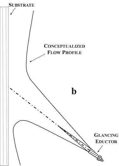 Figure 2 - Schematic representation of glancing eductor configuration and resulting velocity profile.Our electrochemical cell utilizes eductor flow as the primary solution agitation mechanism, but the eductors are positioned beneath the anode chambers behind a dampening element, which directs solution flow across the substrate surface in a more laminar fashion. This laminar flow is facilitated by distinct flow channels formed between the anode chamber and substrate, as shown schematically in Fig. 3. The formation of flow channels has been demonstrated to significantly improve plating uniformity, when compared to deposition in the same cell without flow channels (Fig. 4).12 Plating thickness distribution is quantified by a coefficient of variation (CV), where low CV values are indicative of high thickness uniformity of the electrodeposit.
We have evaluated the plating thickness uniformity of competing cell geometries in order to gauge the benefits of the patented cell technology. In this work, we plated flat stainless steel panels in three plating tanks under DC conditions (25 A/ft2; 2.69 A/dm2). The conditions of these tests are summarized in Table 1 and the results are presented in Fig. 5.8 As seen in Fig. 5, deposits obtained in our cell exhibit a significantly higher level of deposit uniformity when compared to a conventional cell that utilizes air sparging and glancing eductors and a tank representative of current industry practice that utilizes both glancing and impinging eductors. Note that the data presented in Fig. 5 is calculated from points 1.5 in. from the edges of the panel, as is the data presented in Fig. 4.
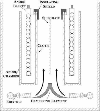 Figure 3 - Schematic side view of the electrochemical cell.
Table 1 - Comparison of varying cell geometries for uniformity studies.
| Cell technology | A:C (mm) | Solution flow | Eductor orientation | Lateral oscillation | Vibration | Knife edge |
| Conventional geometry | 229 | Air sparging eductor | Glancing | 12 cycles/min | N | N |
| Representative geometry | 229 | Eductor | Glancing/impinging | 12 cycles/min | Y | Y |
| Faraday cell | 213 | Eductor | Novel arrangement | 26 cycles/min | Y | N |
In addition to the formation of flow channels formed between the anode chambers and the workpiece, the anode chambers have incorporated insulating shields that further enhance plating uniformity (picture-frame style shielding, shown in Fig. 6). Other shielding may be added to the cell to ensure uniformity of substrates with different dimensions, e.g., a 21×24-in. panel versus the standard 18×24-in. panel, or to address novel plating needs, such as the need for thicker/thinner deposits on certain areas of the panel. In the current work, we explore the effect of insulating shields on the deposit uniformity.
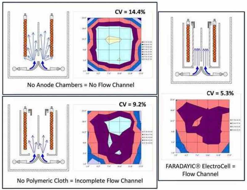 Figure 4 - Thickness distribution as a function of the cell components.
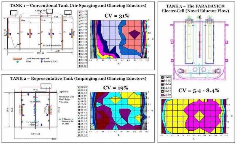 Figure 5 - Results of uniformity studies with the electrochemical cell and competing cell geometries.
Experimental
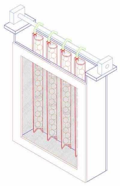 Figure 6 - Anode box geometry with incorporated frameFaraday evaluated the effect of insulating shields on the resulting thickness distributions in our cell using proprietary copper plating chemistry.*** The chemistry was supplied by a commercial partner and, as such, was initially supplied after many hours of use, giving a more industrially relevant data set. The plating tank contained 1700 L of solution and was optimized for an 18×24- in. panel, though substrates of other dimensions were easily accommodated and uniformly metallized. Two 300 L/min. pumps circulated electrolyte through six 19-mm eductors (three on each side) located horizontally under the anode chamber. Vibration of the PCB was accomplished by two horizontal eccentric rotating weights powered by variable speed motors and mounted to each end of the load bar. The frequency of vibration has a range of 0 to 2170 cycles/min. Lateral oscillation was produced by a positive drive from a variable speed motor-reducer with crank arm and linkage. The frequency of oscillation could shift from 6 to 63 cycles/min. with a stroke of 25 mm. Experiments were conducted using a Plating Electronics GmBH Power-Pulse pe 86D-6- 212-480 rectifier. Each plating experiment was conducted under DC conditions of 25 A/ft2 (2.69 A/dm2) for 60 min. The resulting foils were peeled from the stainless steel substrate and measured with a micrometer (Mitutoyo Digimatic Micrometer, Series 293) at thirty-six equispaced points one inch from each side of the panel (pattern shown in Fig. 7). The one-inch measurement protocol was used for these tests to better address manufacturing needs as PCB features are often located one inch from the edges. Three measurements were taken from different areas of measurement point (area diameter of 3⁄8 in.), and averaged for each data point. The measurement borders began one inch from each edge. The measurement points were thus approximately 3.2 in. (x-axis) and 4.4 in. (y-axis) apart.
Table 2 - Summary of tests conducted in the evaluation of insulating shields on thickness uniformity in the Faraday electrochemical cell.
| Test no. | Panel size | Shield opening | Anode spacing | CV (5) |
| 1 | 18×24 in. | No Shield | 3.5 on. | 15.2 |
| 2 | 18×24 in. | 7.5 in. top only | 3.5 on. | 13.2 |
| 3 | 18×24 in. | 7.5 in. top only | 5.5 on. | 8.9 |
| 4 | 18×24 in. | 15×22 in. | 3.5 on. | 10.9 |
| 5 | 18×24 in. | 17×21.75 in. | 3.5 on. | 8.7 |
| 6 | 18×24 in. | 17×21.75 in. | 5.5 on. | 8.5 |
| 7 | 18×24 in. | 17×21.75 in. B | 3.5 on. | 7.4 |
| 8 | 18×24 in. | 18×22.5 in. | 3.5 on. | 11.1 |
| 9 | 18×24 in. | 18×22.5 in. P | 3.5 on. | 15.1 |
| 10 | 21×24 in. | 7.5 in. top only | 5.5 on. | 11.2 |
| 11 | 21×24 in. | 17×21.75 in. | 5.5 on. | 7.5 |
| 12 | 21×24 in. | 18×22.5 in. | 5.5 on. | 9.6 |
| 13 | 21×24 in. | 18×22.5 in. P | 5.5 on. | 9.8 |
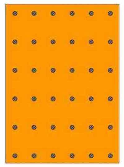 Figure 7 - Measurement protocol for CV calculations. shielding.Tests were conducted using both 18×24-in. and 21×24-in. flat stainless steel substrates as commercial interest revolves around these panel dimensions. Insulating shields (openings of 15×22 in., 17×21.75 in., 18×22.5 in. and 7.5 in.) were constructed from polypropylene. Each pair of shields were secured to the inside of each anode chamber such that the opening for the anode chamber was the same as that of the shield with the exception of the 7.5-in. shield, which provided top shielding only rather than the frame style of the other shields. Use of insulating shields helped to focus current to the center of the panel, minimizing edge effects and improving overall uniformity. Each anode chamber contained four anode baskets with soluble copper anode balls.† For all tests, flow was controlled at 60 gal/min., lateral oscillation at 26 cycles/min. and vibration at 1400 cycles/min. Plating temperature was maintained at 72°F (22°C).
Results
Table 2 summarizes the tests conducted to assess the effect of insulating shields on plating uniformity. As noted in Table 2, the frame described as 17×21.75 in. B is the same shield as 17×21.75 in., except it was installed upside down from 17×21.75 in. and the shield described as 18×22.5 in. P was constructed of perforated polypropylene such that none of the shield was solid polypropylene.
Discussion
As shown in Table 2, the use of insulating shields may have a positive effect on panel uniformity, but experimental optimization is necessary. For example, Fig. 8 is a surface plot of Test 1 (No shield, CV = 15.2%) and Test 7 (17×21.75-in. B panel, CV = 7.4%). The visual difference between these deposits is obvious, and plating at the edges of Test 1 is considerably thicker than that of Test 7.
Furthermore, use of 7.5-in top shielding was more beneficial for Test 3 (18×24-in. panel, CV = 8.9%) when compared to Test 10 (21×24-in panel, CV = 11.2%), when utilizing anode spacing of 5.5 in., as shown in Fig. 9. The spacing of the anode baskets appears to have an effect on thickness distribution in the case of the 7.5-in shield, whereas there appears to be no effect for the frame-style shielding (Tests 5 and 6) presumably due to the presence of side and bottom shields inherent with the frame style shields. This is illustrated in Fig. 10 for Tests 2 and 3 (7.5-in. top shield) and for Tests 5 and 6 (17×21.75-in. frame shield).
Since the effect of anode spacing on thickness uniformity appears to be dependent on shield type/dimension, it can be used to favorably influence deposition of different sized substrates. However, it is anticipated that, in industrial practice, a single spacing protocol would be adopted and, varying substrate dimensions would be addressed through insulating shields. In this manner, our electrochemical cell is flexible in operation, and it is easily adaptable to a wide range of substrate dimensions with simple installation of experimentally optimized insulating shields.
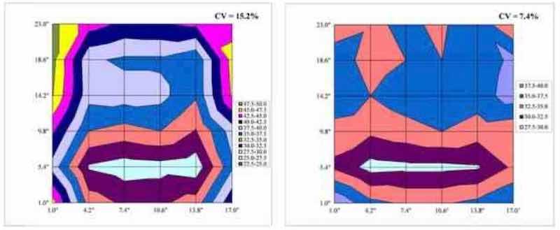 Figure 8 - Surface plots comparing thickness distribution from Test 1 (no shielding, left) and Test 7 (17×21.75-in. frame shield, right).
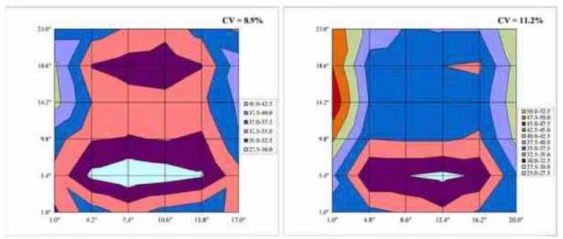 Figure 9 - Surface plots comparing thickness distribution from Test 3 (18×24-in. panel, left) and Test 10 (21×24-in. panel, right), comparing 7.5-in top shielding for different panel sizes.
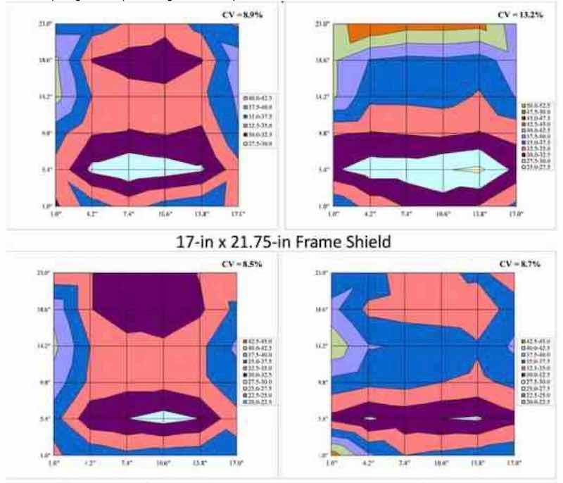 Figure 10 - Comparison of anode basket spacing as a function of shield type (frame or top shielding).
Conclusions
With our novel electrochemical cell, we have developed an efficient tool for the copper metallization of PCB substrates, as well as for many other applications, including electrodeposition of a number of industrially important alloys, electropolishing of highly passive materials like niobium, titanium and nitinol, and electropolishing/electromachining of stainless steel substrates. This technology demonstrates a high level of plating uniformity when compared to conventional and competing cell geometries as well as inherent flexibility for different substrate dimensions with simple installation of insulating shields. Further, it is scalable to meet the needs for research and development tools and full-scale manufacturing lines.
References
1. K.C. Yung, et al., IEEE Trans. Electron. Pack. Manuf., 26 (2), 106 (2003).
2. M. Paunovic & M. Schlesinger, Fundamentals of Electrochemical Deposition, Wiley, Inc., New York, NY (1998).
3. M. Ward, D.R. Gabe & J.N. Crosby, Proc. European PCB Convention, Munich, Germany (1999).
4. P. Dixit, J. Miao & R. Preisser, Electrochem. Solid State Lett., 9 (10), G305 (2006).
5. L.E. Gebhart, et al., “Electroplating Cell with Hydrodynamics Facilitating More Uniform Deposition Across a Workpiece During Plating,” U.S. Patent 7,553,401 (2009).
6. L.E. Gebhart & E. J. Taylor, “Electroplating Cell with Hydrodynamics Facilitating More Uniform Deposition on a Workpiece with Through Holes During Plating,” U.S. Patent Appl. No. 11/836,903 (2007).
7. L. E. Gebhart, et al., “Electroplating Cell with Hydrodynamics Facilitating More Uniform Deposition Across a Workpiece During Plating,” U.S. Patent Appl. No. 12/431,030 (2009).
8. J. Sun, et al., Proc. IPC APEX/Expo, Anaheim, CA (2005).
9. D-T. Chin & C-H. Tsang, J. Electrochem. Soc., 125 (9), 1461 (1978).
10. K-L. Hsueh & D-T. Chin, J. Electrochem. Soc., 133 (1), 75 (1986).
11. K-L. Hsueh & D-T. Chin, J. Electrochem. Soc., 133 (9), 1845 (1986).
12. H.M. Garich, et al., ECS Trans., 19 (26), 11 (2009).
Acknowledgement: Financial support for this work is gratefully acknowledged from the National Science Foundation under Grant No. IIP-1057816.
About the Authors
Information from 2012
Mr. Stephen T. Snyder is a Senior Scientist at Faraday Technology, Inc. Mr. Snyder received his Bachelor of Chemical Engineering degree from the University of Dayton in 2001 and his M.S. degree in Materials Engineering from Purdue University in 2005. He currently directs the design and engineering of cell technology for a variety of electrochemical plating and etching applications. Mr. Snyder has also investigated pulse/pulse reverse processes for electrochemical intercalation of graphite, hydrogen permeation modeling and stainless steel electropolishing.
Ms. Holly M. Garich is a Principal Scientist at Faraday Technology, Inc. Ms. Garich received her B.S. and M.S. degrees in Chemistry from Wright State University in 1999 and 2001, respectively. Currently, she is leading Faraday’s efforts in cell and process design for electrodeposition of copper for printed circuit boards, including build-up and testing of reactors for acid copper rinse water and electropolishing of niobium for superconducting radio frequency cavities. Ms. Garich is a member of the American Chemical Society and NASF.
Mr. Burhanuddin S. Kagajwala is a Senior Scientist at Faraday Technology Inc. Mr. Kagajwala received his B.E. degree in Electronics from Mumbai University in 2008 and his M.S degree from the University of Houston in 2010. His graduate research work was focused on studying the effects of additives in electroplated permalloy (Ni-Fe) films. Currently, he is contributing to different aspects of electrochemistry related to the electroplating of copper, Co-Mn alloys and trivalent chromium, as well as the electroetching of titanium and stainless steel.
Dr. E. Jennings Taylor is the Chief Technical Officer and Intellectual Property Director at Faraday Technology, Inc., Clayton, Ohio. He founded the company to develop and commercialize innovative electrochemical technology using pulse/pulse reverse electric fields. He delivered the William Blum Scientific Achievement award address at SUR/FIN 2008 in Indianapolis, IN. He received his B.A. in Chemistry from Wittenberg University, his M.A. in Technology Strategy and Policy from Boston University, and his M.S. and Ph.D. degrees in Materials Science from the University of Virginia. He has published more than 125 technical papers and articles and holds 30 patents. He serves as Chairman of the AESF Foundation Research Board.