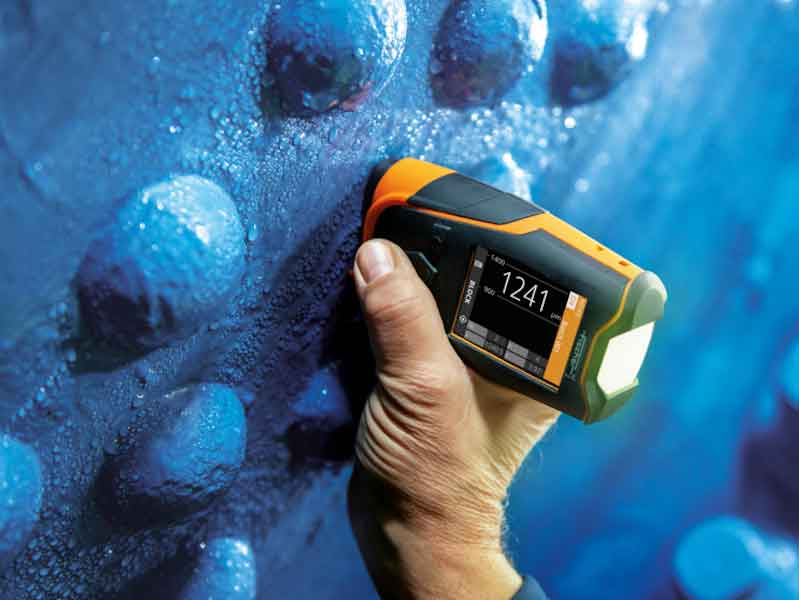
In engineering, a coating is classified as a material that is deposited onto the surface of another material (commonly referred to as a substrate) to specifically enhance the properties of the surface for functional or decorative purposes.
 Kenan HandzicA number of factors dictate the type of coating that would be applied to the material surface which include cost, life of service of the component, substrate the coating is applied to, size and shape of the component, component environment and most importantly the function of the component that is to be coated. Coatings are applied to surfaces according to specific standards, such as ISO, BS, ASTM, DIN etc., additionally, the thickness of the applied coating is dictated by its function and cost. Typical coating thicknesses can range from a few nanometres to several centimetres. As an example, Titanium Zirconium (TiZr) coatings can be 1nm to 5nm thick, while anodic films can range from 0.5μm to 150μm, paint coatings can be up to a couple of millimetres in thickness.
Coatings fall into two distinct categories: layers formed by reactions involving the modification of the surface of the substrate material and those that are deposited on the surface of the substrate material.
- Coatings formed by reactions involving the surface of the substrate tend to form a layer at the substrate surface by chemically acceleration reactions that naturally take place in order to protect the substrate from for example corrosion. Anodising is one of the most notable of these methods which can be used to protect the underlying substrate material.
The latter types of coatings are more varied and offer different properties depending on the coating that is applied to the substrates.
- Most common types of coatings applied to substrates are those applied in solution by a reduction reaction of ions and include electro-deposited coatings (chrome, gold, silver etc) or by electroless deposition methods (eg. Electroless nickel plating). Read more about Electroless Nickel plating measurement
- Other coatings are applied to surfaces “in bulk.” These coatings can be painted or dipped (paint, hot-dip galvanising), or can be welded directly to the surface (cladding or welding overlays).
- Coatings can be deposited on substrates in a liquid state (spray painting or thermal spraying). These coatings tend to further undergo a process once applied to a surface in order to bond. For example, thermally sprayed coatings require cooling from their molten state in order to bond, while solvents are required to evaporate from the paint in order for it to bond with the substrate it is applied to.
- The final type of coatings are those that are deposited by vapour methods (physical and/or chemical vapour deposition [PVD/CVD]). PVD coatings tend to be either solid or liquid and are in deposited on the surface of the substrates by condensation of a vapour on the surface of the substrate or by sputtering. CVD coatings however are applied by heating the substrate to more than 520°C and passing a gas or vapour across the surface of the substrate. Chemical reactions at the surface of the substrate gradually build up a coating which could be a nitride, carbide, oxide or diamond-like carbon.
Why Apply Coating To A Surface?
Coatings are usually applied to a surface tend to be of three types:
Decorative Coatings: Seek to improve the visual appearance of the components they are applied to. Manufactured components such as bathroom fixtures have a chrome or titanium nitride coating applied to raise their visual appeal. Powder coats applied to anodised components, such as window and door frames, tend to again increase the visual appeal of the component they are applied to. It is possible to apply powder coats in many colours to cater the varying requirements customers have for the buildings these components are incorporated into. The paint and lacquer applied to a car body differs between manufacturers and all offer various types of finish to the colour of the vehicle (for example matt, metallic or iridescent/ pearlescent paint finishes). Although these coatings enhance the visual aspects of components, more often than not they also have functional aspects to them.
Functional Coatings: Designed to perform a specific function, protecting the underlying surface, these coatings tend to come in various forms. Nitride based coatings (titanium, niobium or zirconium) are used in the automotive industry to protect surfaces, such as engine or gear components, against frictional stresses acting on these components, while also providing lubricating properties between the components. The various coatings function between 50°C and 400°C or more and still maintain their protective/ lubricating properties, thus increasing component lifetime. Antifouling coatings are used in the marine industry to protect ship hulls from corrosion by sea water. An added benefit to these coatings is that they are smooth and from 80μm up, it is estimated that they save a typical tanker £300,000 on its annual fuel costs (British Coatings Federation, 2020). Sacrificial coatings such as zinc, when applied to steel substrates tend to be preferentially corroded over the steel. During this process, the zinc forms a carbonate film which resists further corrosion efforts on the steel.
Economic: These coatings tend to be a higher value coating applied to surfaces of cheaper base materials for their visual, decorative or functional properties. Accessories such as earrings, rings, necklaces, broaches etc., for the low value market, tend to be manufactured of alloys of copper. The items subsequently have a precious metal coating applied to them (silver or gold) which tend to increase the visual aesthetics of the component but keep the manufacturing costs low. The cost benefits can then be passed to the consumers.
Why Measure Coatings?
Coatings that have functional roles, are usually highly regulated by standards BA, ASTM, DIN, ISO, QUALICOAT, QUALINOD etc. As outlined in the above paragraph coatings performing specific functions have to be regulated. In the example of the TiN coating in the engine, the coatings are applied to strict tolerance limits. Above the specified limits, the coatings would impede the function of the engine components, while below these limits the components may fail without adequate protection from the frictional stresses it is applied for. When components are manufactured the coatings are checked to ensure they are within these parameters; alternatively, coatings can be measured at various intervals during the life of a component, to ensure that they have not been worn away. Coatings wearing away can cause corrosion to occur in the substrate material potentially causing catastrophic failure, especially if that component is used in the automotive, aerospace, rail or marine industries.
A second reason to measure coatings is strictly from a financial standpoint. Current prices of gold, platinum and silver for example, mean that companies that manufacture components with these coatings can be losing money if they add too much of the coating to the components. An example is the electroplated silver on copper wires used in cabling for the aerospace sector. In order to ensure that wires meet the strictest standards for this sector, it may be common to apply more silver to the copper wire, to ensure the wire is in specification. For manufacturers this can translate into an accumulated cost of $250,000 per year in just over-depositing the silver coating. Another example is the automotive industry applying paint and lacquer to the car bodies. By saving 1μm on the paint/ lacquer that is over applied, the manufacturers can save £1 per car. In 2019 approximately 2.3 million cars were registered in the UK, suggesting that a potential of £2.3 Million can be saved per year (Society of Motor Manufacturers and Traders, 2020). Thus, the need to measure the coatings becomes clear.
How To Measure Coatings
So, if coatings are such an important part of our industry, how can they be measured? Broadly, the instruments that measure coatings generally fall into two categories: destructive and non-destructive methods.
Destructive Methods
Destructive methods tend to, as the name suggests, destroy the component in the measurement process. This can occur through the preparation of the sample, as seen with microscopy, or the removal of the coating, as seen with the couloscope (reverse electroplating) method.
Microscopy
Microscopy is a whole topic in itself, but for the purposes of this article, we will concentrate on optical microscopy and electron microscopy. As a technique microscopy requires light to shine on a sample for it to be reflected back to the camera or ocular lenses through a series of magnifying objective lenses, allowing magnification of an image up to 1000x its normal size. The resolution limit of optical microscopy is defined by Abbe’s diffraction limit formula (Equation 1), but typically around 1μm; more than is required to identify the coating-substrate boundary. Organic and inorganic coatings can be measured, as can multiple layers simultaneously.

Equation 1: Abbe’s diffraction limit (d) is calculated by dividing the wavelength of light by 2 times the numerical aperture of the objective lens (n sinθ) commonly written as 2NA.
Optical microscopy relies on the operator to make a judgement on the thickness of the coating normally based on using the software on the microscope. In order for this happen, however, the operator must prepare the sample. In the case of large components, they have to be cut into a more manageable size which would fit on the microscope. The cut components then have to be mounted, cross-sectionally, in an epoxy resin to maintain the component structure/shape. Finally, it is ground and polished to expose the substrate-coating boundary, which can be measured for thickness.
The benefit of this method of inspection is that the samples are tested directly without the need for a coupon. There is also a visual record of the sample after processing which is inspected by the operator to ensure it is of good quality before the thickness is measured.
There are some downsides to testing coating thicknesses in this way. Namely, throughput is low, quality of a sample can be inconsistent due to operator variability, grinding and polishing of the sample can cause smearing of the layers, sample needs to be vertical in the resin and the polishing plane needs to be maintained (if not can cause error in thickness estimation), frequent stops have to be made in order to inspect the sample during polishing therefore can take a long time to prepare the samples. Although an easy to use and highly versatile method for coating thickness measurement, the sample can be destroyed, if not using a coupon, and the low throughput often push people towards other methods to test coating thicknesses.
As with optical microscopy, electron microscopy relies on an adequate cross-section of the sample to be presented in order for the thickness of the coating to be calculated. Instead of using light to interrogate the coating thickness, electron microscopes tend to use electrons to generate a signal from a sample. They can magnify the image to more than 1,000,000 times its size thus enabling the visualisation of grain structure of metals. The samples can be prepared in a similar fashion to optical microscopy.
The benefits of this technique are the increased magnification of the sample making it more accurate. However, in addition to the issues seen with optical microscopy when preparing samples, the cost of these instruments needs to be considered and that the operators need to be highly qualified in order to use them effectively. Microscopy is a diverse topic and other methodologies within the field exist so the most common types have been discussed here.
Couloscope (reverse electroplating)
The couloscope measures the thickness of virtually any metallic coating, including multi-layer, on any substrate material; it works according to the coulometric method by anodic dissolution (DIN EN ISO 2177). This involves dissolving a metal coating off of its metallic or non-metallic substrate by means of an electrolyte under controlled electric current, i.e. reversing the electroplating process (de-plating). The current required for de-plating is directly proportional to the mass of the metal to be removed. A clear correlation between the de-plating time and the coating thickness arises when the test current and area are both kept constant. De-plating takes place in a measuring cell (miniature electrolytic bath). The measuring area is defined by a plastic gasket attached to the measuring cell. The electrolytes used are formulated for the various coating materials such that de-plating does not start until current flows. A pump circulates the liquid within the measuring cell, continually refreshing the electrolyte in contact with the de-plating area, thereby ensuring uniform de-plating. Depending on the size of the area to be measured, gaskets with various diameters can be used for the measuring cell.
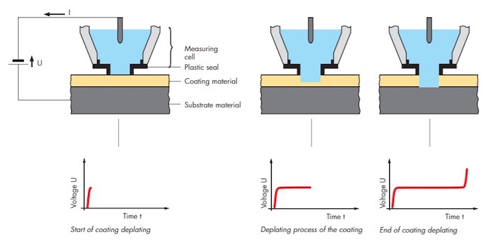
Figure 1: Schematic diagram of the de-plating process. The plating process initiated (left). As the coating is de-plated the voltage reaches a plateau (middle). Once the coating is completely de-plated, the current rises again. The length of time between the initialisation of the process and the end (rise in voltage) is used to calculate the coating thickness.
There are a number of advantages to using a couloscope to measure coating thickness. Multiple coatings can be measured on any substrate, the there is no sample preparation, it is fast and results are accurate (less than 1 μm). However, the method is not without limitations. The method cannot measure non-metallic coatings and the sample is de-plated (it is destructive).
Nanoindentation/ Atomic Force Microscopy (AFM)
Nanoindentation methods are typically used to probe the mechanical properties of samples including coatings. In the Instrumented Indentation Test, an indenter penetrates the specimen’s surface using a specified load F. During this process, the depth of the indentation h is measured continuously. From the penetration depth a number of material properties can be determined including Martens hardness (HM), Vickers hardness (HV)., Elastic modulus of indentation EIT and indentation hardness HIT (Figure 2).
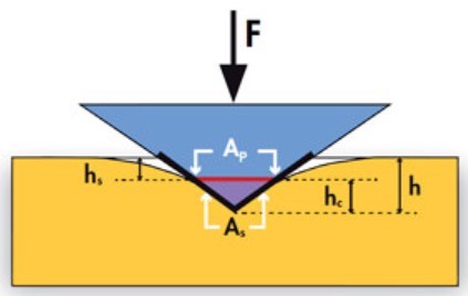
Figure 2: Schematic diagram of the functioning principle of nanoindentation. An indenter is pushed into the surface of the coating at a known force (F) and the depth of the indentation (h) is measured. The contact depth (hc) and elastic displacement (hs) among others are calculated.
Among the other parameters that are generated, the thickness of a coating (more than 1μm) can be calculated from the force curve the instrument generates. Once the indenter penetrates the coating to 10% of the thickness, the effects of the substrate are realised in the force curve. This results in a sharp spike from which the total thickness of the layer can be calculated. For a coating of 10μm in thickness, once the indenter penetrates 1μm into the coating, the change is detected.
An additional, method that can be used to measure coating thickness is the Atomic Force Microscopy. It is included here as it shares similar principles as nanoindentation. AFM relies on a cantilever/ indenter to be brought to the surface of the material and dragged in a straight line across the surface. Any peaks or valleys are detected as the cantilever moves over them. As the cantilever rises due to a peak, a laser aimed at the back of the cantilever is deflected which is converted into a displacement value (thickness). The same principle is true for the valleys. An analogy of the technique would be dragging a finger across a rough surface and feeling the peaks and valleys. The instrument has to have access to the substrate material which it would use as the reference ‘starting’ height.
For coatings and substrates that cannot be measured by tactile methods these are alternative methods that can calculate thickness of coatings. The technique is not limited by the substrate or coating material and although nanoindentation does leave an imprint on the surface of the material AFM does not. Both systems are extremely accurate and offer more information about the coating than just the simple thickness.
One caveat to using such instrumentation is that it can be expensive to acquire. Additionally, the operators have to be highly trained to use AFM and interpret the results. If the substrate materials are metallic then other simpler methods exist to measure coating thickness.
Non-destructive Methods (AFM)
In contrast to the previous methods where the sample is destroyed in order to test the coating thickness, the following methods attempt to measure the coating thickness without destroying the sample.
Ultrasonics
Ultrasonic methods induce sound waves into a material in order to measure its thicknesses. Although primarily used for wall thicknesses, such as those of oil or gas pipes (to detect corrosion on the internal diameters), they can additionally be used to measure the thicknesses of coatings. A sound wave, once introduced into the surface of a material travels towards its opposite side (Figure 3). Any boundaries that the wave passes, for example those between a coating and substrate, result in a reflection of a signal back towards the probe that generated it. This is detected and internally, based on the speed of sound in the material, the thickness is calculated using the formula for distance, speed and time (Equation 2).
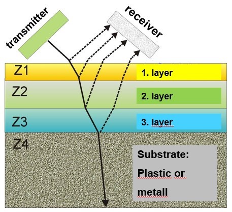
Figure 3: Schematic diagram of a ultrasonic two element probe. The transmitter element sends a sound pulse into the material Z1-Z4. At each layer interface sound is reflected back towards the probe and is detected by the receiver.

Equation 2: Equation used to calculate the thickness of the sample using an ultrasonic gauge. Thickness is calculated by multiplying the speed (of sound in the material) by the time (taken to perform one trip from initial signal to detection of the reflection) and divided by 2.
Ultrasonic methods can be used to measure on almost any material (as long as it is solid). The gauges tend to be small and portable therefore quick to use. They can penetrate deeper into materials than other non-destructive techniques and as a result have applications as flaw detectors to search for flaws, cracks and de-laminations.
As with any technique ultrasonics have their shortcomings. The instruments cannot measure coatings thinner than around 80μm. The equipment tends to require certified technicians to operate. Porous material is difficult to measure as the sound is scattered by voids in the coatings. Finally, surfaces need to be easily accessible and a coupling fluid has to be used to allow the soundwaves to enter the material being tested. Ultimately, ultrasonic devices have been used successfully in the oil and gas industry to detect flaws and corrosion on oil pipelines.
β-Backscatter
Although this technique has largely been replaced by techniques such as XRF (below), it is still one that can be used to measure coating thicknesses. The method measures according to EN ISO 3543 standards of measurement. Briefly, an isotope, located in the probe, emits β-particles which penetrate the surface of the coating and substrate. Particles that are scattered back at 180° from the coating and substrate are detected by a Geiger-Muller counter tube. The coating is only measured successfully if there is a difference of at least 5 atomic numbers between the coating and the substrate.
The β-backscatter has been employed in the automotive industry to measure paint and lacquers on plastic components like bumpers as well as in the electronics industry to measure coatings on ceramics. The strengths of this technique are that it can measure on a large variety of substrates, plastic, glass, metal etc. The method is relatively simple to use and requires minimal training. Conversely, the operators are working with a radioisotope which itself needs to be registered and the regulations around their use is very strict.
Tactile Methods
‘Tactile methods’ is a term generally reserved for measuring techniques that require testing the sample by application of a probe onto the surface of the component. Typically, two methods fall into this category and are referred to as the magnetic induction or eddy current methods.
Magnetic Induction
The magnetic induction method is one specifically utilised for coatings on ferromagnetic substrates. The schematic diagram below (Figure 4) shows how an excitation current (I~) generates a low-frequency magnetic field with a strength proportional to the distance between the probe and the base material. A measurement coil measures the resulting magnetic field. The obtained measurement signal is converted into the coating thickness values using a characteristic probe output function (normally specific to manufacturers).
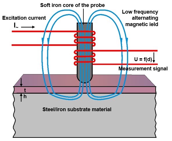
Figure 4: Schematic diagram of a probe utilising the magnetic induction method to measure the thickness of a coating on a ferromagnetic substrate. The thickness of the coating dictates the current and subsequent magnetic field generated. The change in current/ magnetic field is measured by a secondary coil around the probe tip and converts the raw data values to a coating thickness.
Typical applications include non-ferrous metal, organic plastic/ paint coatings or anodic films on electrically conductive non-ferrous metal substrates. Industries such as architectural (anodising), automotive (dry film thickness of paint) and aerospace (functional or protective coatings on lightweight substrates) are some examples of where this technique is utilised for coating measurements. Much like magnetic induction, the technique fast, accurate and requires minimal training to use effectively. The factors influencing the eddy current technique will be discussed (below).
Other Tactile Methods
Three additional techniques are used for more complex or specialised applications. The first of these methodologies is the Hall effect method utilising the Lorentz force. The Lorentz force creates a potential difference between two sides of a sample that can be measured as the Hall voltage and subsequently the thickness calculated from it. It is typically suitable for ferromagnetic material on non-ferromagnetic substrates.
Another method is the Eddy Current (phase sensitive) method. The method relies on a phase shift between the excitation and detection signals in order to calculate the coating thickness. ‘Phase-Eddy’ is interesting as it can measure dual coatings (eg paint on zinc, copper or nickel) on ferromagnetic substrates such as steel, but also has the ability to measure organic coatings on non-ferromagnetic substrates.
Finally, the resistance measurement method is used to measure Ohmic resistance using a four-pole probe. This method is specifically used to measure non-ferromagnetic coatings on organic substrates; for example, copper on epoxy resin in PCB manufacturing.
Factors Influencing Tactile Measurements
Three additional techniques are used for more complex or specialised applications and more information can be found by following this link: The first of these methodologies is the Hall effect method utilising the Lorentz force. The Lorentz force creates a potential difference between two sides of a sample that can be measured as the Hall voltage and subsequently the thickness calculated from it. It is typically suitable for ferromagnetic material on non-ferromagnetic substrates. Another method is the Eddy Current (phase sensitive) method. The method relies on a phase shift between the excitation and detection signals in order to calculate the coating thickness. ‘Phase-Eddy’ is interesting as it can measure dual coatings (eg paint on zinc, copper or nickel) on ferromagnetic substrates such as steel, but also has the ability to measure organic coatings on non-ferromagnetic substrates. Finally, the resistance measurement method is used to measure Ohmic resistance using a four-pole probe. This method is specifically used to measure non-ferromagnetic coatings on organic substrates; for example, copper on epoxy resin in PCB manufacturing.
Shape of Specimen
Sample curvature, size and thickness all influence the readings in this category.
Instruments are typically calibrated on flat surfaces of the uncoated components to be measured. This constitutes a baseline reading for the instruments. If subsequent parts to be measured are also flat then the shape is not an issue. If the components are curved, however, this can pose an initial problem in getting accurate measurements. Calibration on a flat specimen, and subsequent measurements on a convex component geometry, results in a thickness reading greater than nominal. Conversely, measuring on a concave component geometry results in a measurement that is thinner than nominal (Figure 6).
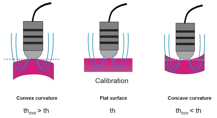
Figure 6: Schematic diagram of the measurement on convex (left), flat (middle) and concave (right) surfaces. Calibration on a flat surface and measurement on a convex component results in thickness reading than nominal, while measurement on concave components results in a thinner than nominal thickness reading.
There are methods for eliminating the effects of curvature on readings. The first of these is to calibrate the instrument on each surface that will be measured and acquire the measurements. As this is a long and laborious process it is also possible to use higher end instruments which can have a number of applications and have a calibration for each of these applications. The measurements are then performed using the specific previously calibrated application. A third method for circumventing the effects of curvature is to use a curvature compensating probe (for example FTD3.3 probe manufactured by Helmut Fischer GmbH). Using this probe, it is possible to calibrate on a flat surface and measure convex components accurately.
Another factor to consider is the size of the measurement area. Tactile probes require a minimum area in order to make accurate measurements. Calibrating on a large area and measuring in a smaller area can increase the reported thickness of the sample measured and increase the spread of the readings. This can be particularly problematic when measuring close to the edge of a component (Figure 7).
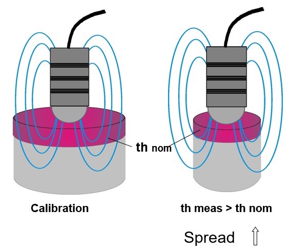
Figure 7: Schematic diagram of a probe calibrated on a large surface and measuring on smaller surfaces. The magnetic field generated by the probe, is influenced by the substrate air boundaries at different points which increases the reported thickness readings.
One way to overcome this issue is to use a stand to calibrate the instrument on the smaller surface prior to applying the coating. The use of the measurement stand ensures that the probe is positioned in the identical area from one component to the next. This minimises the spread of the readings and gives more accurate results. Another way to overcome this issue is to use a probe with a smaller diameter magnetic field (by lowering the operating frequency), but this could have other potential issues.
The final factor is the thickness of the substrate material. Here issues arise when a device is calibrated on a thick substrate and subsequent measurements are acquired on much thinner substrate components (Figure 8). The resulting measurement results tend to be higher than nominal and the spread of the results increases.
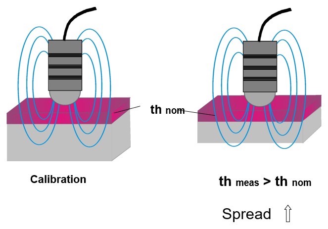
Figure 8: Schematic diagram of a probe calibrated on a thick substrate and measurements performed on thin substrate components. The magnetic field penetrates through the substrate when upon reaching the substrate-air interface it is deflected. The measured coatings appear thicker than the nominal value.
The issues are easily overcome by using a probe with a higher frequency which increases the size of the magnetic field (lateral) but decreases its depth within the substrate. Alternatively, the instrument can be calibrated on the thinner substrate thus eliminating its effects.
Substrate and Coating Material
Two issues are commonly seen that are elicited by the substrate or coating and have an effect on the measurements. They are roughness and substrate conductivity.
The roughness of the substrate and coating can have a large influence on the ability of the instrument to measure accurately. For quite rough surfaces, the probe tip may rest on the peaks or in the troughs and as such cause variation in the readings that may result in the component not passing quality control (Figure 9).
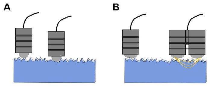
Figure 9: Schematic diagram depicting how substrate roughness can affect probe positioning and subsequent thickness measurements (A). Larger diameter probe tip and dual pole probes used as alternative probes for eliminating influence of roughness.
Placing the probe on the peaks or troughs can have dramatic differences on the coating thickness measurements. Calibration in this instance is not always going to solve the issue, but probes with larger diameter probe tips that rest on the peaks is one possible solution to the issue. Another solution is the possibility of using two pole probes, which generate the magnetic fields between the two poles thus averaging the roughness and rectifying the problems encountered.
The electrical conductivity of the substrate is the other problem encountered when measuring coatings. Calibrating an instrument on a substrate, such as brass (conductivity at 58 MS/m) and measuring components with significantly different conductivities, such as titanium (conductivity at 1.5 MS/m), results in significantly thicker readings measured (Figure 10).
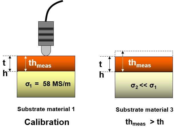
Figure 10: Schematic diagram of the influence of substrate conductivity on coating thickness measurements.
Certain probes, such as the FTA3.3 probe [Helmut Fischer GmbH], is able to compensate for some differences in electrical conductivity, for example brass (58MS/m), aluminium (45MS/m) and copper (58.6 MS/m) it still has difficulties changing to titanium (1.5MS/m). To overcome the issue, one simply must calibrate on the new substrate and measure.
Instrument Properties
Apart from the instruments needing annual calibration to ensure that they are functioning correctly, the only issue with the instrument that can affect the readings is probe tip ware. For eddy current methodologies, this is not an issue as the probe tip is manufactured from poor electrically conducting materials. For magnetic induction methods, the influence is great since the probe tip has to conduct the magnetic field.
A possible solution is to a worn probe tip is to simply calibrate the instrument again, however, this does not fix the issue entirely as the readings would drift further as the wear on the tip progresses further. Only solution for this issue is to change probe tip itself which can be cheaper than replacing the entire probe.
Operator Expertise
Operators can influence the thickness of coatings by placing the probe at an angle onto the surface of the coating or alternatively indenting the coating through applying too much pressure.
The tilting issue is mainly reserved to probes with large or a flat measurement tip as the rotation is not around the magnetic symmetry axis (Figure 11).
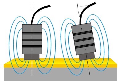
Figure 11: Schematic diagram depicting the tilting effect that an operator could have on coating thickness measurements.
The tilting effect can be eliminated by offering further training to the operators. Alternatively, a measurement stand can be acquired such as the V12 Motorised stand [Helmut Fischer GmbH].
The issue of indentation is apparent in both magnetic induction and eddy current methods but through different means. Magnetic induction reads a thinner coating than nominal only when the coating is physically compressed. Eddy currents, however, tend to pool inside a dent once the substrate material is indented by the probe tip.
To overcome the issue of indentation, it is possible to use spring loaded probes to remove some pressure the tip exerts on the surface of the material. Additionally, an automated stand can alleviate all excess pressure by modulating the approach speed when contacting the coating surface.
External Influences
There are three external factors that can affect the measurements made magnetic induction or eddy current methods. The first is a strong magnetic field (alternating electromagnetic field or constant magnetic field). Alternating EM field can be negated by using appropriate shielding while constant magnetic fields act directly on the probe and thus instrument use should be avoided in these areas.
Temperature is the next factor to consider. Components in excess of 80°C can melt the glue holding the probe and force the components to expand causing alterations in the magnetic field frequency. An additional consideration is that at higher temperatures the coatings and substrates also expand, which could result in false coating thickness readings and potential failures (below specification) once components cool. These issues can be avoided by using a probe designed for measuring at higher temperatures, or by simply allowing the component to cool before performing any measurements.
The final external factor that could affect probe readings is measurements made on components with an excess of aggressive liquids, acids or bases used in electroplating or anodising. Moisture-proof probes can be used to avoid liquid ingress or alternatively components can pat dried prior to measuring.
XRF
XRF relies on the fundamental principle that when an energy source excites individual atoms, the atoms emit energy or a wavelength of light, characteristic of the atom it originated from. By analysing the number of photons of each energy, samples may be segregated into their composition elements and from this information the coating thickness and elemental composition can be calculated.
The ability of XRF to distinguish between different atoms makes it an incredibly powerful technique in the analysis of multi-layers (theoretically up to 24 with SDD detectors and if the coatings are thin enough to allow the signal through), also it can be used to measure the thickness of alloyed material coatings. XRF does require more training than tactile methodologies, and readings tend to take longer than 5 seconds.
In the silicon wafer semiconductor manufacturing industry, coatings tend to be stacked, and XRF is used to routinely measure 5 to 10 layers simultaneously. XRF also does posses the ability to interrogate the composition of a coating (for example the ratio and thickness of a zinc-nickel coating) or even the percentage pf phosphorous in a nickel-phosphorous layer.
Conclusions
These are just a number of techniques that are utilised in industry to measure coating thickness others do exist but are beyond the scope of this article. The techniques presented here are a guide and the benefits/ drawbacks of each technique have been presented. Ultimately it is important to contact a representative from a company that manufactures coating thickness instrumentation to discuss a solution that best fits ones needs.
Kenan Handzic is the Service Excellence Manager at Fischer Instrumentation (GB) Ltd in Worcester, England, United Kingdom. Please visit www.fischer-technology.com


