


The cross-sectional microstructure, local chemical composition, and mechanical behavior of anodic oxide layers produced by oxalic acid anodizing of cast A356 aluminum alloy were investigated using digital optical microscopy, scanning electron microscopy (SEM), energy-dispersive X-ray spectroscopy (EDS), and in situ nanoindentation inside the SEM chamber.
 Alexandra Musza, Dávid Ugi, Nguyen Quang Chinh, and Ádám Vida.The anodized specimens contained a compact oxide-side interfacial region adjacent to the substrate–oxide interface and an outer porous oxide layer. The oxide layers formed at the higher nominal charge density were generally thicker than those formed at the lower charge density. Cross-sectional nanoindentation revealed two characteristic interface-related features: localized, unusually high apparent hardness values on the oxide side of the interface and a gradual hardness increase within the adjacent substrate-side region.
The highest apparent values exceeded the expected hardness range of anodic oxide layers on A356 alloy and were therefore interpreted as interface-affected responses rather than intrinsic oxide hardness values. Their repeated occurrence at a well-defined position nevertheless supported their association with the oxide-side interfacial region. The substrate-side hardness increase was characterized by the estimated width of an anodizing-affected substrate zone. EDS line scans showed that the oxide-side interfacial region retained a significant oxygen concentration, whereas the substrate-side hardness increase was not accompanied by a systematic elemental concentration gradient.
The results demonstrate that the cross-sectional mechanical response of oxalic-acid-anodized A356 alloy is governed not only by the conventional barrier-layer–porous-layer structure, oxide thickness, and porosity, but also by local chemical composition, microstructural heterogeneity, and substrate/interface-related effects.
1. Introduction
Aluminum and its alloys are widely used as structural materials because of their low density, favorable strength-to-weight ratio, and good castability. These properties are particularly advantageous in the automotive and aerospace industries, where weight reduction contributes to improved energy efficiency and lower environmental impact. However, material selection based on favorable bulk properties does not necessarily guarantee adequate surface performance under demanding service conditions. Intensive wear, sliding contact, and prolonged exposure to aggressive environments may cause surface degradation even when the bulk material retains sufficient structural performance. Surface modification is therefore frequently applied to improve surface hardness, wear resistance, corrosion resistance, and service life without sacrificing the advantageous bulk properties of the alloy [1,2].
During anodizing in acidic electrolytes, the anodic oxide film generally develops a duplex structure composed of a compact barrier layer adjacent to the metal and an outer porous oxide layer. The porous layer is commonly described as a cellular structure, in which approximately hexagonal oxide cells contain pores at their centers. These pores are usually oriented approximately perpendicular to the substrate surface. The morphology, thickness, and functional properties of the anodic oxide layer are strongly affected by the anodizing parameters, including electrolyte composition, applied current density or voltage, bath temperature, and treatment time. In addition to these processing parameters, the microstructure and chemical heterogeneity of the starting alloy can also influence local oxide growth and dissolution behavior. Under galvanostatic conditions, oxide growth is therefore related to the transferred charge density, which depends jointly on the applied current density and anodizing time [3,4].
The type of electrolyte plays a decisive role in determining the resulting oxide morphology and properties. Sulfuric acid, oxalic acid, and phosphoric acid electrolytes are among the most frequently used acidic baths for aluminum anodizing, but they produce oxide films with different pore dimensions, growth rates, dissolution behavior, and mechanical characteristics. In addition to these conventional electrolytes, other carboxylic-acid-based systems have also been investigated. For example, anodizing in malonic acid solution has been shown to produce characteristic voltage-charge responses and porous anodic oxide films whose morphology depends strongly on current density and electrolyte composition [5]. However, such systems differ from oxalic-acid anodizing in electrolyte chemistry and electrochemical response; therefore, they provide useful background for the broader sensitivity of anodic oxide growth to anodizing conditions, rather than a direct quantitative reference for the present A356/oxalic-acid system. Under carefully controlled conditions, oxalic-acid anodizing can produce relatively regular porous morphologies, particularly on high-purity aluminum. However, morphological regularity should not be interpreted as complete chemical, structural, or mechanical homogeneity. The uniformity of the resulting oxide also depends strongly on substrate composition and microstructure, surface preparation, electrolyte concentration, temperature, current density, and treatment time [6,7,8,9].
The structural model of porous anodic alumina was fundamentally described by Keller et al. [10], who introduced the concept of a porous cellular oxide structure and a compact barrier layer at the metal side of the film. This model is highly useful for understanding anodic oxide formation on aluminum. However, the anodizing behavior of aluminum alloys is more complex than that of high-purity aluminum. Alloying elements, intermetallic particles, and second-phase constituents can locally disturb the electric field, oxide growth rate, dissolution process, and ion transport through the forming oxide [11,12,13,14]. These effects are particularly important for cast Al–Si–Mg alloys such as A356, where eutectic Si particles, Mg-containing phases, and other microstructural inhomogeneities are present in the aluminum matrix. Such heterogeneities may modify not only the local morphology and continuity of the oxide layer, but also its chemical composition and local mechanical response.
Accordingly, the anodic oxide formed on cast A356 alloy should be regarded as locally heterogeneous rather than as a chemically and morphologically uniform layer. Eutectic Si particles and Mg-containing or other second-phase regions may react differently from the aluminum matrix during anodizing, producing local variations in oxide growth, film thickness, pore morphology, continuity, composition, and mechanical response [15,16,17,18]. These local variations are important because the mechanical response measured in cross-section is not determined only by the average oxide thickness or by the general porous-layer morphology. Instead, the measured hardness may also reflect the local structure and chemistry of the oxide, the proximity of the substrate–oxide interface, and the microstructural features inherited from the cast alloy.
The mechanical behavior of anodic oxide layers is strongly influenced by their layered and porous structure. The compact oxide-side interfacial region near the substrate–oxide interface may respond differently from the outer porous layer, where pores reduce the effective load-bearing cross-section. Previous studies have shown that the hardness and mechanical resistance of anodic oxide layers are closely connected to pore structure, crack formation, oxide compactness, and degree of porosity [19,20,21,22]. More generally, the mechanical response of porous alumina-containing systems is also sensitive to pore architecture and interfacial constraint. For example, Ghorbanhossaini et al. demonstrated in resin composites containing milled anodic porous alumina that filler geometry and filler–matrix interactions significantly influence elastic modulus and strength [23]. Although this system differs from anodized A356 alloy, it further illustrates that the mechanical response of porous alumina-containing materials can be strongly affected by local architecture and interface-related effects.
In addition to the oxide-side response, the substrate-side region directly adjacent to the oxide layer may also be affected by the anodizing process. Cross-sectional nanoindentation can reveal gradual changes in hardness near the substrate–oxide interface even when the indentation position is located on the substrate side. In the present work, this mechanically affected substrate-side region is referred to as the anodizing-affected substrate zone (AASZ). This term is used to distinguish it from the oxide-side interfacial region and from the barrier layer. The AASZ is not treated as a separate layer and is not identified with the barrier layer; rather, it denotes the substrate-side region where the hardness response changes when approaching the anodized oxide layer.
The present work builds on our previous research on oxalic-acid-anodized A356 alloy [24], but addresses a different aspect of the anodized system. Whereas the previous study reported the general surface morphology and hardness behavior of anodic films formed on A356 alloy, the present work focuses on oxide-layer heterogeneity and the spatially resolved mechanical response across the substrate–oxide interface. The purpose of this study was not to optimize the anodizing process or to establish general oxide-growth kinetics, but to use selected anodizing conditions to produce oxide layers with different thicknesses and cross-sectional morphologies suitable for interface-resolved characterization. Low-temperature galvanostatic anodizing was used to limit chemical dissolution while directly controlling the current density. Current densities of 2 and 6 A/dm2 were selected to represent lower- and higher-current conditions under the same treatment duration. Thus, the selected conditions were intended to support cross-sectional analysis of oxide-layer heterogeneity and interface-related mechanical response rather than to establish an industrially optimized anodizing process.
Accordingly, the aim of this study was to characterize oxide-layer heterogeneity and to determine the interface-resolved cross-sectional hardness response of oxalic-acid-anodized cast A356 alloy. Oxide-layer thickness and morphology were evaluated together with position-resolved in situ nanoindentation profiles and EDS line scans. This combined approach was used to distinguish the oxide-side near-interface apparent hardness maxima from the gradual hardness change within the adjacent anodizing-affected substrate zone and to relate both features to the local chemical and microstructural environment.
2. Materials and Methods
2.1. Sample Preparation and Anodizing
The substrate used in this study was a cast A356 aluminum alloy with a nominal chemical specimen composition of Al–7Si–0.29Mg (wt.%). The material was supplied by an industrial partner in Spain within the framework of a previous research project. Rectangular specimens with nominal dimensions of 60 mm × 40 mm × 10 mm were used. The specimens were fully immersed during anodizing, and a nominal total external surface area of 0.68 dm2, calculated from the specimen dimensions, was used to determine the applied current. Prior to anodizing, the surfaces intended for treatment and subsequent characterization were mechanically prepared by grinding with SiC abrasive papers in the P80–P2500 grit range, followed by polishing with a 7 µm alumina-based polishing paste. The SiC abrasive papers and alumina-based metallographic consumables were supplied by Struers ApS (Ballerup, Denmark). The mechanically prepared specimens were then immersed for 50 min at room temperature in a 20 g/L aqueous pretreatment bath prepared in-house using a commercially available phosphate-containing cleaning formulation. The concentration and treatment time were selected on the basis of preliminary experiments performed on the same material system. After pretreatment, the specimens were rinsed with laboratory-produced distilled water and an 80 vol.% aqueous ethanol solution prepared in-house.
The anodizing-cell configuration was based on the setup described previously [24] and is shown schematically in Figure 1. The fully immersed specimen served as the anode and was connected to the positive terminal of a DC power supply. An aluminum cathode with a surface area approximately three times that of the specimen was connected to the negative terminal. The anode–cathode distance was maintained at approximately 6 cm. Electrical contact with the specimen was established by tightly inserting an aluminum wire into a central drilled hole in the. The diameter of the wire was selected to match the diameter of the hole, allowing mechanical fixation by direct metal-to-metal contact between the wire and the specimen. No screw, bolt, clamp, or additional metallic fastener was used in the electrolyte. The aluminum wire was covered with an insulating polymer tube along its immersed length, and the tube was positioned as close as possible to the specimen surface. This arrangement was intended to prevent direct exposure of the connecting wire to the electrolyte while maintaining electrical contact inside the drilled hole. Since no separate metallic fixture was exposed to the electrolyte, no additional fixture area was included in the anodizing-area calculation. The nominal current density was calculated using the geometric external specimen area of 0.68 dm2. Accordingly, the applied currents were 1.36 and 4.08 A for nominal current densities of 2 and 6 A/dm2, respectively.
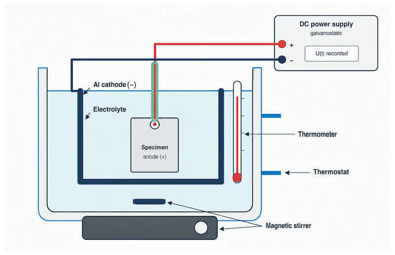
Figure 1. Schematic representation of the anodizing setup and the electrically insulated specimen-contact arrangement.
Anodizing was carried out under galvanostatic conditions in an aqueous electrolyte containing 70 g/L technical-grade oxalic acid dihydrate (H2C2O4·2H2O), corresponding to 0.56 mol/L. The bath temperature was maintained at 10 °C using a thermostatic cooling system (Julabo F25, JULABO GmbH, Seelbach, Germany), continuously monitored with a thermometer, and the electrolyte was stirred at 200 rpm to improve temperature and concentration uniformity. The parameters were selected based on preliminary experiments and our previous study on the same material system [24]. The relatively low temperature was used to limit chemical dissolution of the growing oxide layer and to reduce electrolyte heating, particularly at the higher current density. Galvanostatic operation provided direct control of the applied current density. Current densities of 2 and 6 A/dm2 were selected as two contrasting conditions previously investigated on this material system. The lower value represented the reference condition, whereas 6 A/dm2 was deliberately selected to promote more pronounced porous-oxide development. The purpose was not to establish an industrially optimized anodizing process or to analyze anodizing kinetics, but to investigate oxide-layer formation and interface-related mechanical behavior under the selected preparation conditions. A treatment time of 60 min was used for all specimens to obtain oxide layers sufficiently developed for position-resolved cross-sectional characterization. Sample M1 was anodized at 2 A/dm2 for 60 min, while samples M2–M5 were anodized at 6 A/dm2 for 60 min. Samples M1, M2, and M4 were left unsealed, whereas samples M3 and M5 were subjected to hydrothermal pore sealing in hot distilled water. Accordingly, M2 and M4 represent nominally identical unsealed conditions, while M3 and M5 represent nominally identical sealed conditions. The limited specimen series was used to assess sample-to-sample variation associated with the heterogeneous microstructure of the cast A356 alloy and was not intended as a formal process-reproducibility study. The pore-sealing procedure was selected based on previous studies performed on the same material system [24]. The cell voltage was recorded manually at approximately 5 min intervals during galvanostatic anodizing to document the overall cell-voltage response under the selected preparation conditions.
After anodizing and, where applicable, hydrothermal sealing, cross-sectional slices were prepared using a diamond cutting wheel. The cross-sectional surfaces were prepared separately for SEM, EDS, and nanoindentation analyses by grinding with SiC abrasive papers in the P320–P2500 grit range and polishing to a mirror finish using a 1 µm alumina-based polishing slurry supplied by Struers ApS (Ballerup, Denmark). Finally, the specimens were rinsed with laboratory-produced distilled water and dried with warm air.
2.2. Surface and Cross-Sectional Characterization
The microstructure of the A356 base alloy and the oxide layers formed by anodizing was examined using digital optical microscopy (VHX-2000, Keyence Corporation, Osaka, Japan) and scanning electron microscopy (Quanta 3D FEG, FEI Company, Hillsboro, OR, USA) equipped with an integrated EDS system. Cross-sectional SEM observations were performed at accelerating voltages of 10–30 kV, depending on the imaging mode and magnification. Secondary electron (SE) and backscattered electron (BSE) imaging modes were used to characterize the oxide-layer morphology, cross-sectional continuity, and contrast variations near the substrate–oxide interface.
Metallographically prepared cross-sections were used to evaluate the thickness, continuity, and morphology of the oxide layers. The mean oxide-layer thickness was determined from calibrated digital optical micrographs using 20 spatially separated measurements along the cross-section of each specimen. The optical micrographs presented in the manuscript show representative local regions of the corresponding cross-sections; therefore, local thickness values measured only within the displayed field of view may differ from the statistical mean values reported in Table 1.
Table 1. Anodizing conditions, calculated nominal charge densities, average oxide-layer thicknesses, and estimated widths of the anodizing-affected substrate zone.
| Sample | Current Density j (A/dm2) | Anodizing Time t (h) | Charge Density q (C/cm2) | Sealing | Average Oxide-Layer Thickness; d (µm) | AASZ Width x0 (µm) |
| M1 | 2 | 1 | 72 | No | 41.0 ± 5.3 | 44.6 |
| M2 | 6 | 1 | 216 | No | 124.3 ± 12.0 | 4.3 |
| M3 | 6 | 1 | 216 | Yes | 108.3 ± 2.1 | 4.8 |
| M4 | 6 | 1 | 216 | No | 110.3 ± 12.2 | 3.0 |
| M5 | 6 | 1 | 216 | Yes | 98.0 ± 8.6 | 7.8 |
Local chemical composition was investigated using EDS line scans across selected cross-sectional regions. The distributions of Al, O, Si, and Mg were determined across the oxide layer, the substrate–oxide interface, and the adjacent substrate-side region. The EDS profiles were evaluated together with the cross-sectional hardness profiles to distinguish the oxide-side interfacial region from the adjacent substrate-side region and to assess whether the substrate-side hardness increase was accompanied by systematic compositional changes.
2.3. In-Situ Nanoindentation Measurements
In situ cross-sectional nanoindentation measurements were performed using a mobile nanoindenter integrated into an SEM chamber, which enabled precise positioning and direct observation of the indentations. A Berkovich diamond tip was used. The displacement and load resolutions of the system were approximately 1 nm and 1 µN, respectively. Further details of the experimental setup are provided in Ref. [25].
Force was determined from the deflection of a leaf spring monitored by a capacitive displacement detector. Before testing, the spring-deflection signal was calibrated against displacements observed directly by SEM, and the spring constant was determined using reference weights. The measurements were performed using the device-specific platen-velocity-control mode, without electronic feedback control of load or penetration depth. The commanded velocity ranged from 20 to 60 nm/s, with 60 nm/s used for samples M2–M5. The indenter was held at the terminal position for 20 s before unloading. Because of the strongly varying local mechanical response across the substrate–oxide system, neither a fixed maximum load nor a fixed maximum penetration depth was prescribed. The resulting maximum forces ranged from 3.0 to 22.8 mN, while the characteristic contact depths were typically approximately 0.10–0.80 µm. Hardness was determined using the Oliver–Pharr method [26,27].
The indentations were positioned along the polished cross-section from the substrate toward the oxide layer. Between 25 and 42 valid, spatially distinct indentations were evaluated per specimen. The measurements therefore represented position-resolved hardness profiles rather than a predefined number of repeated indentations within each microstructural region. The experimental setup is shown in Figure 2.
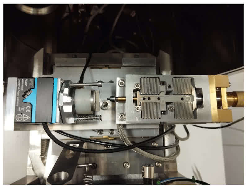
Figure 2. Mobile nanoindenter integrated into the SEM chamber used for the in situ cross-sectional nanoindentation measurements.
3. Results and Discussion
3.1. Anodizing Response, Oxide Layer Thickness and Morphology
The cell-voltage records obtained during galvanostatic anodizing are shown in Figure 3. The records document the overall macroscopic response of the anodizing cell under the selected preparation conditions. Since the voltage values were recorded manually at approximately 5 min intervals, the curves are not used for quantitative modelling of oxide-growth kinetics or for identifying detailed transition regions. Instead, they are presented to document the applied galvanostatic treatments. The interpretation of the anodized specimens is based on oxide-layer thickness, cross-sectional morphology, EDS line scans, and in situ nanoindentation results.
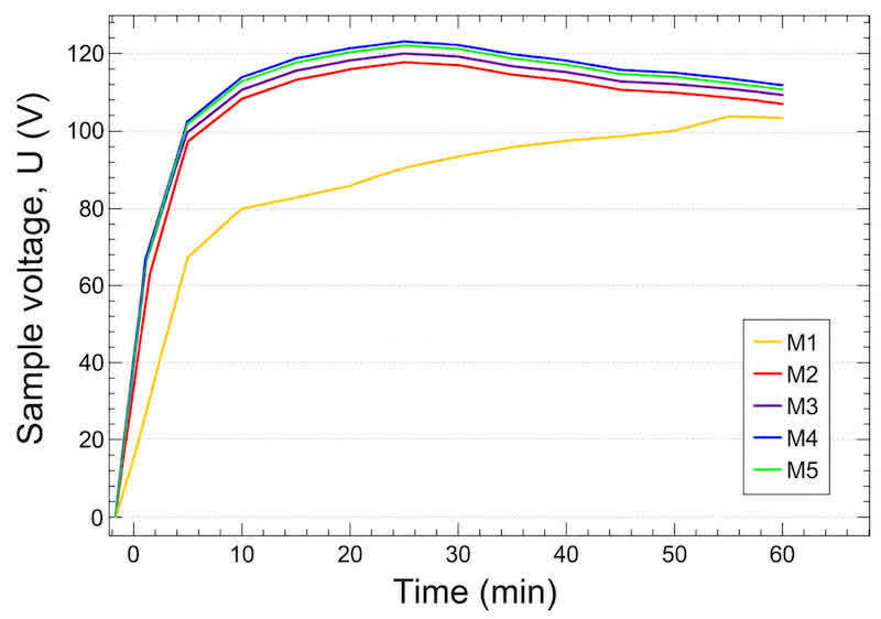
Figure 3. Cell-voltage records obtained during galvanostatic anodizing of the evaluated samples. The voltage values were recorded manually at approximately 5 min intervals. The records document the overall macroscopic cell response under the selected preparation conditions and are not used for quantitative modelling of oxide-growth kinetics.
The measured oxide-layer thicknesses are summarized in Table 1 together with the applied anodizing conditions, calculated nominal charge densities, and estimated widths of the anodizing-affected substrate zone, denoted as x0. In this work, x0 is used as a descriptive parameter for the substrate-side region in which the indentation response begins to change near the substrate–oxide interface. The x0 values were obtained from the hardness-profile fitting described in Section 3.2 and should not be interpreted as the thickness of the barrier layer or as a distinct intermediate layer.
The nominal charge densities were 72 C/cm2 for M1 and 216 C/cm2 for M2–M5. M1, anodized at the lower current density, exhibited a mean oxide-layer thickness of 41.0 µm, while samples M2–M5, anodized at the higher current density, exhibited thicknesses between 98.0 and 124.3 µm. Among the samples treated under nominally identical anodizing conditions, some thickness variation remained. Because of the limited specimen series and the heterogeneous cast microstructure, the independent effects of sealing, local substrate heterogeneity, and sample-to-sample variation cannot be quantified separately.
Cross-sectional SEM observations revealed an oxide structure consisting of an outer porous layer and a compact oxide-side interfacial region adjacent to the substrate–oxide interface. Figure 4 shows representative cross-sectional SEM characterization of the anodized A356 system. Figure 4a presents a low-magnification cross-sectional SEM image of the unsealed M2 specimen, showing the A356 substrate, the oxide-side interfacial region, and the anodic oxide layer. Figure 4b shows the representative nanoindentation measurement geometry across the substrate–oxide system. The observed local variations in oxide-layer thickness and morphology are consistent with the heterogeneous microstructure of cast A356 and the associated spatial differences in oxide growth [13,15,18].
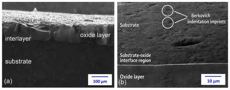
Figure 4. Representative cross-sectional SEM characterization of the anodized A356 sample: (a) oxide layer and substrate–oxide interface showing the main cross-sectional regions used for interpretation; (b) representative nanoindentation measurement geometry across the substrate–oxide system. The combined figure illustrates the spatial relationship between the oxide layer, the substrate–oxide interface, and the indentation positions used for the cross-sectional hardness evaluation.
Representative cross-sectional digital optical micrographs of samples M1–M5 are presented in Figure 5. The images were selected from the cross-sectional datasets used for thickness evaluation and are intended to illustrate the overall layer morphology and local thickness variations. All scale bars represent 100 µm. The oxide-layer thickness values reported in Table 1 are statistical mean values calculated from 20 spatially separated measurements performed over a broader cross-sectional region of each specimen. Therefore, thickness values measured only within the displayed field of view of a representative micrograph may differ from the mean values reported in Table 1. This is particularly relevant for cast A356 alloy, where local microstructural heterogeneity can lead to variations in oxide growth and layer thickness along the cross-section. Specimens M3 and M5 were subjected to hydrothermal pore sealing after anodizing. Since no dedicated morphological investigation of the sealing effect was performed, the present results are not used to quantify sealing-induced changes in oxide morphology or thickness. Sealing is considered only as an additional processing difference when interpreting the cross-sectional hardness profiles.
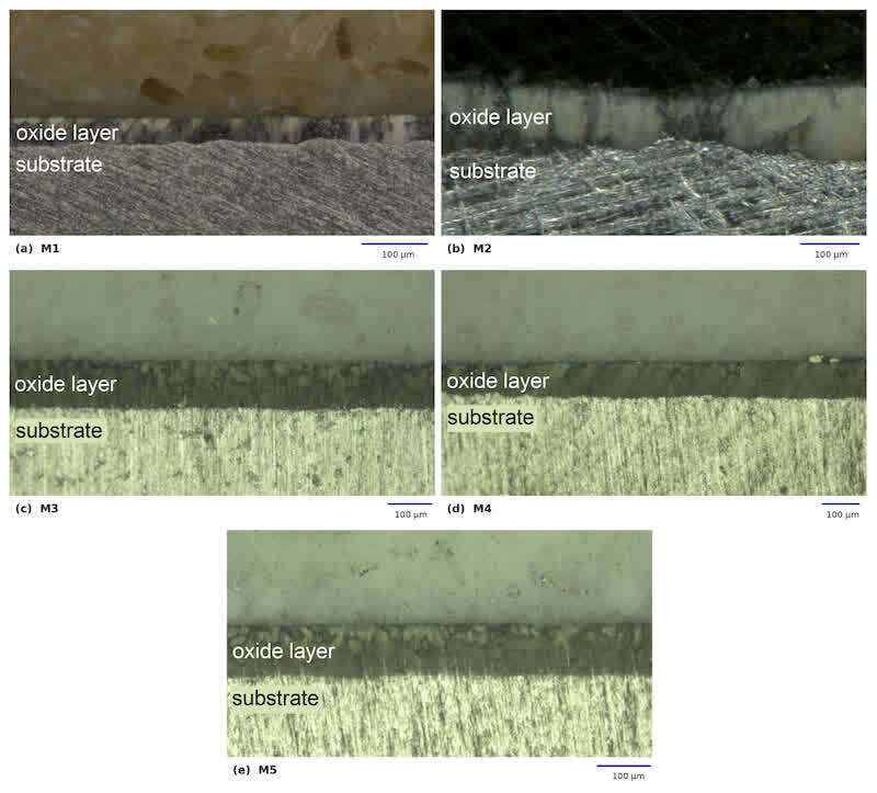
Figure 5. Representative cross-sectional digital optical micrographs of samples (a) M1, (b) M2, (c) M3, (d) M4, and (e) M5 used for the oxide-layer thickness evaluation. All scale bars represent 100 µm.
3.2. Interface-Related Indentation Response in the Cross-Sectional Profiles
In our previous work, cross-sectional in situ nanoindentation measurements on an oxalic-acid-anodized A356 sample revealed a pronounced hardness increase near the substrate–oxide interface, from the substrate side toward the anodized oxide layer [24]. This initial observation suggested that the local mechanical response near the interface cannot be interpreted solely as the difference between the average properties of the bulk substrate and the porous oxide layer. In the present study, this phenomenon was examined systematically on several anodized samples with different oxide-layer thicknesses and pore-sealing conditions to determine whether the interface-related response is a sample-specific feature or a more general characteristic of oxalic-acid-anodized A356 oxide layers.
Figure 6 shows that the hardness profiles are strongly position-dependent near the substrate–oxide interface. Distances are given relative to the substrate–oxide interface, where d = 0 corresponds to the interface. Positive distances correspond to indentation points on the substrate side, whereas negative distances correspond to indentation points within the anodic oxide layer. This signed-distance convention is also used for the EDS profiles discussed in Section 3.3. Away from the interface, the substrate-side values remained relatively low and stable. In contrast, several oxide-side data points exhibited pronounced localized hardness maxima in the near-interface region. Toward the free surface of the oxide layer, the hardness gradually decreased, consistent with the increasingly porous character of the outer oxide layer and with the hardness decrease reported for hard-anodized aluminum alloys in previous cross-sectional nanoindentation studies [28].
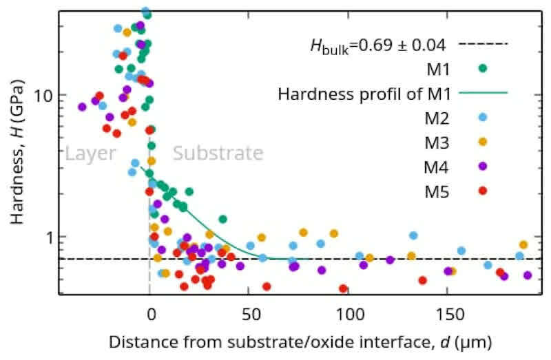
Figure 6. Cross-sectional hardness profiles of the anodized A356 samples measured by in situ nanoindentation. Distances are given relative to the substrate–oxide interface, where d = 0 corresponds to the interface; positive values correspond to the substrate side, while negative values indicate the oxide-layer side. The figure highlights both the strongly increased oxide-side near-interface hardness values and the gradual substrate-side hardness increase approaching the interface. The dashed horizontal line represents the hardness of the unaffected substrate, Hbulk. The inset shows the empirical fitting used to estimate the width of the anodizing-affected substrate zone, x0.
In addition to the localized oxide-side maxima, the substrate-side portions of the hardness profiles showed a gradual increase in hardness when approaching the substrate–oxide interface. This increase was particularly pronounced for M1, where the indentation positions were located on the substrate side and the plastically deformed volume was expected to remain within the substrate material. The substrate region adjacent to the anodic oxide layer was therefore considered to be mechanically affected by the anodizing process. In the present work, this region is referred to as the anodizing-affected substrate zone (AASZ). For the other specimens, the estimated AASZ width was considerably smaller, as shown in Table 1. In these cases, the indentation positions associated with the substrate-side hardness increase were located close to the substrate–oxide interface, and the plastically deformed volume may have overlapped with the adjacent oxide layer. Although the characteristic contact depths were submicrometric, typically approximately 0.10–0.80 µm, the corresponding deformation zone extended beyond the nominal contact depth and may have overlapped with the adjacent oxide layer for indentations positioned close to the interface.
To estimate the AASZ width, the substrate-side hardness data were evaluated as a function of distance from the substrate–oxide interface. The fitting procedure was used only as an empirical estimate and was not intended to represent a physical model of deformation, oxide growth, or substrate modification. For this fitting, d denotes the distance measured from the substrate–oxide interface into the substrate; therefore, the fitting was applied only to positive values of d. The hardness profile was described by the following piecewise function:
𝐻(d)=𝑎(𝑑−𝑥0)3+𝐻𝑏𝑢𝑙𝑘 for 0<𝑑<𝑥0, (1)
𝐻(d)=𝐻𝑏𝑢𝑙𝑘 for 𝑑≥𝑥0 (2)
where Hbulk is the hardness of the unaffected substrate measured far from the substrate–oxide interface, and x0 is the fitted parameter representing the estimated width of the anodizing-affected substrate zone, and a is an empirical fitting coefficient. The Hbulk value was determined from substrate hardness measurements performed at distances greater than 100 µm from the substrate–oxide interface. Thus, x0 represents the distance beyond which the substrate-side hardness values no longer show a systematic change related to the interface. It should not be interpreted as the thickness of the barrier layer or as the thickness of a distinct intermediate layer.
The high oxide-side near-interface values should not be attributed solely to the intrinsic hardness of the barrier layer, because the barrier layer is expected to be much thinner than the characteristic deformation volume involved in nanoindentation. Instead, these values are more consistently interpreted as a combined interface-related indentation response affected by substrate/interface effects, indentation geometry, the compact oxide-side interfacial region, local porosity, residual stresses, and microstructural heterogeneity. The repeated occurrence of the hardness maxima at a well-defined oxide-side position indicates that the phenomenon is not adequately explained by random measurement error. Nevertheless, their magnitude is unusual when compared with literature data. For example, Alcalá et al. [29] investigated barrier-type amorphous anodic alumina films by nanoindentation and reported a hardness of approximately 8.5 GPa. This difference does not invalidate the observed spatial trend, but it shows that values approaching 70–100 GPa cannot be interpreted uncritically as the unconstrained bulk hardness of anodic alumina.
Several factors may contribute to the locally increased indentation response near the substrate–oxide interface. Residual stress generated during anodizing is one possible contributing factor. Çapraz et al. [30] monitored stress changes during the growth and dissolution of anodic oxide films on aluminum using phase-shifting curvature interferometry and showed that significant stress changes can develop during anodic film formation. Although their study was performed on aluminum in phosphoric acid, it supports the view that anodizing-induced stresses may influence the local mechanical response near the metal–oxide interface. In the present samples, the compact oxide-side interfacial region is also expected to be denser and less porous than the outer porous layer, resulting in greater local resistance to deformation. Furthermore, indentation close to the substrate–oxide interface produces a deformation zone constrained by neighboring regions. The measured hardness may therefore represent a combined interface-related response rather than the intrinsic hardness of a single homogeneous phase. Elastic recovery after unloading may additionally reduce the dimensions of the residual impression used to determine the projected contact area, thereby increasing the calculated hardness. Accordingly, the high values are interpreted here as localized oxide-side apparent hardness maxima and not as direct hardness values of the barrier layer alone.
At the same time, the gradual substrate-side hardness increase suggests that the substrate adjacent to the oxide layer may also be affected by anodizing-related structural or mechanically relevant changes. These two effects are complementary: the oxide-side apparent hardness maxima describe the local response of the oxide-side interfacial region, whereas x0 characterizes the estimated width of the anodizing-affected substrate zone. The EDS line scan results discussed in the following section were used to examine whether these interface-related hardness changes are accompanied by local compositional variations.
3.3. Local Compositional Effects on the Interface-Related Indentation Response
The hardness profiles presented in Section 3.2 showed that the highest localized hardness values were not measured in the bulk substrate, but on the oxide side adjacent to the substrate–oxide interface. In addition, the substrate-side profiles indicated the presence of an anodizing-affected substrate zone. To interpret these interface-related features, the microstructural and chemical heterogeneity of the A356 alloy must be considered. In the Al–Si–Mg cast alloy, eutectic Si regions, Mg-containing phases, and other second-phase particles in the substrate can locally modify the growth, composition, and morphology of the oxide layer. Consequently, the region near the substrate–oxide interface cannot be regarded as chemically or mechanically homogeneous. EDS line-scan measurements were therefore performed to examine the local compositional environment associated with the interface-related indentation response.
Figure 7 shows a representative EDS analysis of M2. Figure 7a presents the cross-sectional SEM/EDS image of the region near the substrate–oxide interface and indicates the position of the d–d′ line along which the EDS line scan was measured. Figure 7b presents the corresponding Al, O, Si, and Mg concentration profiles. The compositional changes shown in the graph therefore correspond directly to the microstructural path marked in the image, extending from the oxide layer across the substrate–oxide interface and into the substrate. As shown in Figure 7b, the variation in the Al and O signals clearly identifies the transition from the oxide layer to the substrate. On the oxide-layer side, the oxygen content remains high, while the aluminum content is lower than in the bulk substrate. Across the substrate–oxide interface, the oxygen content decreases markedly, and the aluminum content increases sharply. On the substrate side, the Al content reaches the high level characteristic of the bulk alloy. Local fluctuations in the Si and Mg signals indicate that the distribution of alloying elements is not homogeneous near the interface, which is consistent with the microstructural heterogeneity visible in the SEM/EDS image.
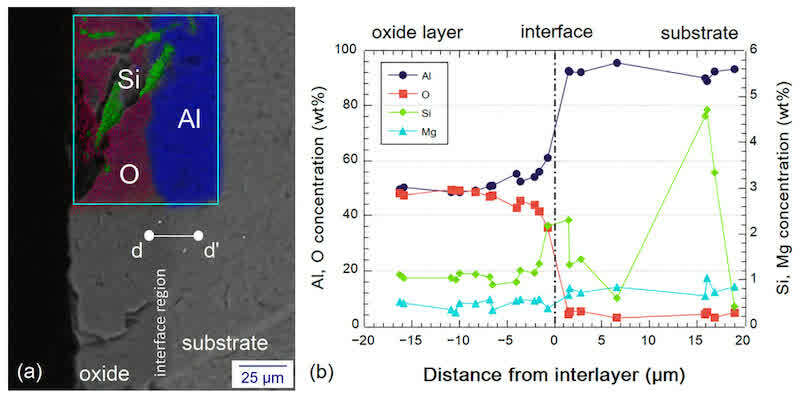
Figure 7. EDS analysis of the anodized M2 sample: (a) cross-sectional SEM/EDS image showing the region near the substrate–oxide interface and the d–d′ line used for the EDS line scan; (b) EDS line scan measured along d–d′, showing the elemental distribution from the oxide layer, across the substrate–oxide interface, and into the substrate. Al and O concentrations are plotted on the left axis, while Si and Mg concentrations are plotted on the right axis. The dashed vertical line at d = 0 indicates the substrate–oxide interface; negative distances correspond to the oxide-layer side, while positive distances correspond to the substrate side.
In addition to the representative M2 profile, the positions of the outlying hardness values were compared with EDS line-scan profiles for the M1 and M3 samples. In each case, the position of the substrate–oxide interface was defined using the steep transition in the EDS Al/O profile as a reference point. The near-interface hardness values were then assigned to the corresponding regions of the EDS profile relative to this reference. Representative values for the three samples are summarized in Table 2. Negative distances correspond to the oxide-layer side of the substrate–oxide interface. Values above 20 GPa were classified as localized high-hardness measurements. They were retained in the spatial profiles and used to evaluate the location of the interface-related response but were not included in the representative hardness evaluation of the outer porous oxide layer.
Table 2. Representative spatial correlation of localized high-hardness measurements with the local EDS composition near the substrate–oxide interface.
| Sample | Distance From Substrate–Oxide Interface d (µm) | HOutlying (GPa) | O (wt.%) | Mg (wt.%) | Al (wt.%) | Si (wt.%) |
| M1 | −1.0 | 36.56 | ~38.6 | ~0.4 | ~59.2 | ~1.0 |
| M2 | −3.6 | 99.26 | ~45.3 | ~0.6 | ~52.4 | ~1.2 |
| M3 | −2.97 | 69.67 | ~46.5 | ~0.5 | ~51.5 | ~1.1 |
Table 2 demonstrates that the localized high-hardness measurements in all three examined samples were associated with the oxide-side interfacial region. At the relevant positions, the oxygen concentration remained high, approximately 38.6–46.5 wt.%, whereas the aluminum concentration remained at approximately 51.5–59.2 wt.% and had not reached the approximately 90–97 wt.% level characteristic of the substrate. By contrast, on the positive-distance substrate side, the hardness decreased toward the range characteristic of the A356 substrate. Together with the common coordinate convention used in Figure 6 and Figure 7, this compositional evidence supports that the pronounced hardness maxima were localized on the oxide side rather than being substrate measurements incorrectly assigned to the oxide layer.
The EDS–hardness correlation supports the non-random spatial association of the localized hardness maxima with an oxygen-rich, chemically and structurally transitional oxide-side region. EDS alone, however, cannot determine whether the absolute magnitude of the indentation response represents intrinsic hardening or includes contributions from local constraint, residual stress, elastic recovery, indentation geometry, and microstructural heterogeneity. The compositional evidence therefore supports the location and repeatedly observed mechanical response, while the values approaching 70–100 GPa are conservatively described as localized oxide-side apparent hardness maxima.
The presence of Si-containing second-phase particles may be particularly important because these particles exhibit electrochemical behavior different from that of the aluminum matrix and can locally affect oxide-film thickness, continuity, and pore structure. Mg-containing regions may also be relevant to ion transport, oxide incorporation, and dissolution processes. These local compositional and structural variations may contribute to the interface-related indentation response observed in the oxide-side region near the interface. Comparison with the EDS profiles also indicates that the substrate-side hardness increase described by the AASZ width, x0, was not accompanied by a systematic elemental concentration gradient in the examined line scans. This finding suggests that the substrate-side component of the interface-related indentation response is not governed by a simple compositional transition alone. Instead, it is more likely related to local structural changes, residual-stress effects, or mechanical constraint near the substrate–oxide interface. Since Table 2 includes representative localized high-hardness measurements only for M1, M2, and M3, the present EDS comparison does not provide an independent basis for evaluating the effect of hydrothermal sealing on the near-interface hardness profiles of all sealed samples.
Overall, the results show that the cross-sectional mechanical response of the anodized oxide layer formed on A356 alloy cannot be interpreted solely in terms of barrier-layer/porous-layer structure, oxide-layer thickness, or porosity. Local composition, second-phase particles, variations in oxide growth, residual stress, and substrate/interface constraint must also be considered. Most importantly, the EDS comparison supports the systematic localization of the pronounced hardness response within the oxygen-rich oxide-side interfacial region. It does not by itself establish values of 70–100 GPa as the unconstrained intrinsic hardness of anodic alumina; rather, it supports their interpretation as repeatedly observed, localized oxide-side apparent hardness maxima.
4. Conclusions
Oxalic-acid anodizing produced porous anodic oxide layers with a compact oxide-side interfacial region on cast A356 alloy. The oxide layers were generally thicker in the samples anodized at the higher current density. Thickness variations were also observed among samples treated under nominally identical conditions, indicating the important role of the heterogeneous Al–Si–Mg substrate and locally nonuniform oxide growth.
Cross-sectional in situ nanoindentation revealed repeatedly occurring oxide-side apparent hardness maxima near the substrate–oxide interface, whereas no comparable values were observed in the bulk substrate. These localized responses were retained for spatial analysis but excluded from the representative hardness evaluation of the outer porous oxide layer. Their magnitude should not be interpreted as the unconstrained intrinsic hardness of the anodic oxide or of the barrier layer alone. Instead, the measured response close to the interface may include contributions from the compact and less porous oxide-side interfacial region, residual stress, mechanical constraint, elastic recovery, indentation geometry, local porosity, and chemical or microstructural heterogeneity. Accordingly, these measurements are interpreted as repeatedly observed, localized oxide-side apparent hardness maxima.
In addition to the oxide-side response, the substrate-side hardness profiles indicated an anodizing-affected substrate zone (AASZ). This zone is distinct from the compact oxide-side interfacial region and should not be interpreted as the barrier layer or as a separate intermediate layer. The AASZ was substantially wider in M1, which was anodized at the lower current density and exhibited the thinnest oxide layer, than in the samples anodized at the higher current density. Since the EDS profiles did not reveal a corresponding systematic elemental concentration gradient, the substrate-side hardness increase cannot be explained by a simple compositional transition alone. Anodizing-induced structural changes, residual-stress effects, and interface-related mechanical constraint remain possible contributions, although their individual roles could not be separated in the present study.
Overall, the combined nanoindentation and EDS results demonstrate that oxide-layer heterogeneity and interface-resolved hardness are closely related in oxalic-acid-anodized cast A356 alloy. Consequently, the cross-sectional mechanical behavior of anodized cast A356 alloy cannot be interpreted solely in terms of oxide-layer thickness, porosity, or the conventional barrier-layer/porous-layer structure. Local composition, second-phase particles, oxide-growth heterogeneity, residual stress, and substrate/interface constraint must also be considered.
Written by Alexandra Musza,1,2,3 Dávid Ugi2, Nguyen Quang Chinh2, and Ádám Vida1,3
1: Materials and Technologies Division, Bay Zoltán Nonprofit Ltd. for Applied Research, H 1116 Budapest, Hungary
2: Department of Materials Physics, Eötvös Loránd University, H 1117 Budapest, Hungary
3: Edortech Ltd., H 1116 Budapest, Hungary
Author Contributions: Conceptualization, A.M. and Á.V.; formal analysis, N.Q.C.; investigation, A.M., Á.V. and D.U.; data curation, A.M., Á.V. and D.U.; writing—original draft preparation, A.M. and Á.V.; writing—review and editing, Á.V. and N.Q.C.; supervision, Á.V. and N.Q.C. All authors have read and agreed to the published version of the manuscript.
Funding: The APC was funded by Bay Zoltán Nonprofit Ltd.
Institutional Review Board Statement: Not applicable.
Informed Consent Statement: Not applicable.
Data Availability Statement: The raw data supporting the conclusions of this article will be made available by the authors on request.
Acknowledgments: During the preparation of this manuscript, the author used ChatGPT (OpenAI, GPT-5.5 Thinking) for language editing. The author reviewed and edited all AI-assisted outputs and takes full responsibility for the content of this publication. D.U. was supported by project no. 146795-PD, implemented with the support provided by the Ministry of Culture and Innovation from the National Research, Development and Innovation Fund, financed under the NKFIH-PD funding scheme. D.U. was also supported by the János Bolyai Research Scholarship of the Hungarian Academy of Sciences.
Conflicts of Interest: Author Alexandra Musza and Ádám Vida was employed by the company Edortech Ltd.. The remaining authors declare that the research was conducted in the absence of any commercial or financial relationships that could be construed as a potential conflict of interest.
Abbreviations: The following abbreviations are used in this manuscript:
- SEM Scanning Electron Microscope
- EDS Energy-Dispersive X-ray Spectroscopy
- AASZ Anodizing-affected substrate zone
References
- Thompson, G. Porous anodic alumina: Fabrication, characterization and applications. Thin Solid Films 1997, 297, 192–201.
- Wernick, S.; Pinner, R.; Mason, R.B. The Surface Treatment and Finishing of Aluminium and Its Alloys. J. Electrochem. Soc. 1957, 104, 180C.
- O’SUllivan, J.P.; Wood, G.C. The morphology and mechanism of formation of porous anodic films on aluminium. Proc. R. Soc. London Ser. A Math. Phys. Sci. 1970, 317, 511–543.
- Masuda, H.; Fukuda, K. Ordered Metal Nanohole Arrays Made by a Two-Step Replication of Honeycomb Structures of Anodic Alumina. Science 1995, 268, 1466–1468.
- Poznyak, A.; Knörnschild, G.; Karoza, A.; Norek, M.; Pligovka, A. Peculiar Porous Aluminum Oxide Films Produced via Electrochemical Anodizing in Malonic Acid Solution with Arsenazo-I Additive. Materials 2021, 14, 5118.
- Masuda, H.; Yamada, H.; Satoh, M.; Asoh, H.; Nakao, M.; Tamamura, T. Highly ordered nanochannel-array architecture in anodic alumina. Appl. Phys. Lett. 1997, 71, 2770–2772.
- Lee, J.; Kim, Y.; Jung, U.; Chung, W. Thermal conductivity of anodized aluminum oxide layer: The effect of electrolyte and temperature. Mater. Chem. Phys. 2013, 141, 680–685.
- Lee, S.; Kim, D.; Kim, Y.; Jung, U.; Chung, W. Effect of aluminum anodizing in phosphoric acid electrolyte on adhesion strength and thermal performance. Met. Mater. Int. 2016, 22, 20–25.
- Chowdhury, P.; Thomas, A.N.; Sharma, M.; Barshilia, H.C. An approach for in situ measurement of anode temperature during the growth of self-ordered nanoporous anodic alumina thin films: Influence of Joule heating on pore microstructure. Electrochim. Acta 2014, 115, 657–664.
- Keller, F.; Hunter, M.S.; Robinson, D.L. Structural Features of Oxide Coatings on Aluminum. J. Electrochem. Soc. 1953, 100, 411–419.
- Zhang, J.-S.; Zhao, X.-H.; Zuo, Y.; Xiong, J.-P. The bonding strength and corrosion resistance of aluminum alloy by anodizing treatment in a phosphoric acid modified boric acid/sulfuric acid bath. Surf. Coat. Technol. 2008, 202, 3149–3156.
- Xu, Y.; Thompson, G.; Wood, G.; Bethune, B. Anion incorporation and migration during barrier film formation on aluminium. Corros. Sci. 1987, 27, 83–102.
- Habazaki, H.; Shimizu, K.; Skeldon, P.; Thompson, G.E.; Wood, G.C.; Zhou, X. Effects of Alloying Elements in Anodizing of Aluminium. Trans. IMF 1997, 75, 18–23.
- Hughes, A.E.; Birbilis, N.; Mol, J.M.; Garcia, S.J.; Zhou, X.; Thompson, G.E. High Strength Al-Alloys: Microstructure, Corrosion and Principles of Protection. In Recent Trends in Processing and Degradation of Aluminium Alloys; Ahmad, Z., Ed.; InTech: London, UK, 2011; pp. 223–262.
- Fratila-Apachitei, L.; Terryn, H.; Skeldon, P.; Thompson, G.; Duszczyk, J.; Katgerman, L. Influence of substrate microstructure on the growth of anodic oxide layers. Electrochim. Acta 2004, 49, 1127–1140.
- Feliu, S.; González, J.A.; López, V.; Bartolome, M.J.; Escudero, E.; Otero, E. Characterisation of porous and barrier layers of anodic oxides on different aluminium alloys. J. Appl. Electrochem. 2007, 37, 1027–1037. [Green Version]
- Tsangaraki-Kaplanoglou, I.; Theohari, S.; Dimogerontakis, T.; Wang, Y.-M.; Kuo, H.-H.; Kia, S. Effect of alloy types on the anodizing process of aluminum. Surf. Coat. Technol. 2006, 200, 2634–2641.
- Razzouk, E.; Koncz-Horváth, D.; Török, T.I. Microstructure Effects on Anodizing High-Silicon Aluminium Alloy AlSi12Cu1(Fe) under Various Surface Conditions and Power Modes. Crystals 2024, 14, 352.
- Garcia-Vergara, S.; Skeldon, P.; Thompson, G.; Habazaki, H. A flow model of porous anodic film growth on aluminium. Electrochim. Acta 2006, 52, 681–687.
- Liu, X.Z.; Yang, J.H.; Wang, G.; Song, L.L.; Zhuang, G.S. Effect of Preparation Conditions on the Performance of Anodic Aluminum Oxide Films. Appl. Mech. Mater. 2012, 164, 223–226.
- Zhao, X.; Liu, W.; Zuo, Y.; Yang, L. The cracking behaviors of anodic films on 1050 and 2024 aluminum alloys after heating up to 300 °C. J. Alloys Compd. 2009, 479, 473–479.
- Zhang, P.; Zuo, Y. Effects of pore parameters on performance of anodic film on 2024 aluminum alloy. Mater. Chem. Phys. 2019, 231, 9–20.
- Ghorbanhossaini, A.; Rafiee, R.; Pligovka, A.; Salerno, M. Dental composites with strength after aging improved by using anodic nanoporous fillers: Experimental results, modeling, and simulations. Eng. Comput. 2022, 39, 387–398.
- Musza, A.; Ugi, D.; Vida, Á.; Chinh, N.Q. Study of Anodic Film’s Surface and Hardness on A356 Aluminum Alloys, Using Scanning Electron Microscope and In-Situ Nanoindentation. Coatings 2022, 12, 1528.
- Ispánovity, P.D.; Ugi, D.; Péterffy, G.; Knapek, M.; Kalácska, S.; Tüzes, D.; Dankházi, Z.; Máthis, K.; Chmelík, F.; Groma, I. Dislocation avalanches are like earthquakes on the micron scale. Nat. Commun. 2022, 13, 1975.
- Pharr, G.; Oliver, W.; Brotzen, F. On the generality of the relationship among contact stiffness, contact area, and elastic modulus during indentation. J. Mater. Res. 1992, 7, 613–617.
- Oliver, W.C.; Pharr, G.M. An improved technique for determining hardness and elastic modulus using load and displacement sensing indentation experiments. J. Mater. Res. 1992, 7, 1564–1583.
- Sieber, M.; Morgenstern, R.; Scharf, I.; Lampke, T. Effect of Nitric and Oxalic Acid Addition on Hard Anodizing of AlCu4Mg1 in Sulphuric Acid. Metals 2018, 8, 139.
- Alcalá, G.; Mato, S.; Skeldon, P.; Thompson, G.; Mann, A.; Habazaki, H.; Shimizu, K. Mechanical properties of barrier-type anodic alumina films using nanoindentation. Surf. Coat. Technol. 2003, 173, 293–298.
- Çapraz, Ö.Ö.; Shrotriya, P.; Hebert, K.R. Measurement of Stress Changes during Growth and Dissolution of Anodic Oxide Films on Aluminum. J. Electrochem. Soc. 2014, 161, D256–D262.