
This study successfully demonstrated the overall advantages of multistep anodization of heat-treated wrought aluminum alloy AA7075-T6 that is a widely used in aerospace, automotive and fracture-critical applications.
The coating properties and morphology are studied in detail for four anodization regimes: a conventional R1 with a constant electric current and R2, R3, R4 with raising the current in two, four and eight steps, respectively. Whereas processes R1 and R2 form coatings with the atomic Al/O ratio of 0.53 that is smaller than 0.67 for oxide Al2O3, R3 and R4 create coatings with the Al/O ratio of 0.83. Due to a higher level of infused oxygen, coatings built in R1 and R2 have burns and powdery appearance, while coatings formed in processes R3 and R4 form exhibit smooth solid-like surfaces. Compared to R1 and R2, R3 and R4 increase the overall growth rate of oxides by 23.4% and 25.6%, respectively, reduce the pore size by 94% and 45% respectively and decrease by 8.4% the amount of a transferred electric charge per one micrometer of the layer thickness. Process R4 creates coatings that are 74.0% more resistant to abrasion, 14.6% harder and 25.4% thicker than coatings formed in R1. As no specialized equipment is required, presented regimes of multistep anodization are well suited for large-scale manufacturing.
1. Introduction
 Peter Totaro and Boris KhusidAnodizing is an electrochemical method used to transform aluminum to aluminum oxide in the coating layer. Although being thin, this layer can substantially increase the abrasion and corrosion resistance of aluminum [[1], [2], [3]]. Aluminum alloys are complexed with zinc, copper and other alloying elements to provide high mechanical strength have relatively low abrasion and corrosion resistance [[3], [4], [5], [6]]. Thus, they are usually anodized to improve abrasion and corrosion resistance [7]. The major difficulty in anodizing these alloys is related to the compositional heterogeneity that is even more accentuated in heat-treatable alloys in which an increase in mechanical strength is achieved by forming several intermetallic precipitates [3,[8], [9]]. The presence of intermetallic compounds facilitates the appearance of defects during anodization by generating a spatially non-uniform distribution of electric current in the alloy matrix. It leads to uneven growth of anodic oxides and surface burning, especially when higher voltages and current densities are applied [3,[10], [11], [12], [13]]. The burning of film is caused by a runaway dissolution at the oxide surface that occurs when the current density is locally spiked. Spikes in the current density, loose powdery coating, insufficient micro adhesion, and evolution of oxygen gas bubbles at the oxide surface are all common issues that decrease the anodization efficiency and are exacerbated by anodizing at higher voltages and currents [8,[13], [14], [15], [16], [17], [18], [19], [20]].
While surface electro-chemical reactions forming the oxide layer are governed by the current density, application of a voltage is required to run the anodization process [3,8,21]. Since the electric resistance of aluminum oxides is much higher than that of aluminum alloys, the anodizing current drastically decreases with time at a constant applied voltage [6,10,13,22]. However, the use of a high voltage for the entire process would significantly raise chances of burning the oxide surface. A compensation approach is to run the entire process at median voltages [21]. However, this strategy does not allow for a large surface area load, increases the energy usage by requiring a larger tank time needed per load, and still brings a higher rate of forming processing defects, especially in anodization of heat-treatable aluminum alloys. This approach is therefore problematic as the appearance of processing defects typically would cause scraping of a metal part, which can be exceedingly costly due to the lead time, machining labor and material cost put into it. Accordingly, these anodizing regimes are of limited use in an industry where profit margins are typically low.
Several recent studies demonstrated that the use of “stepwise anodization,” a process by raising the magnitude of an applied voltage or an electric current during anodization [8,23] can improve surface properties of heat- treatable aluminum alloys, but the outcome was found to strongly depend on various factors, such as the alloy composition, bath type and temperature [[24], [25]]. In stepwise anodizing, the voltage is incrementally increased overtime until the final current or voltage is reached, thereby allowing the use of a lower initial voltage to start the process. It is believed that the use of lower initial voltages and current densities allows non‑aluminum ions to migrate out of the forming aluminum oxide [26] and/or dissolve in an electrolyte when an electric current is applied [27]. In these studies, anodization was controlled by voltage or by current accompanied with voltage pulses. While pulsing can improve mechanical properties of anodized coatings [13,[28], [29], [30], [31]], the cost of required equipment is too expensive on a large industrial scale. Other studies on improvement of anodization of heat-treatable aluminum alloys rely on adding chemical compounds into an anodizing electrolyte and/or changing the temperature to influence the coating formation. Due to the cost and industry restrictions, some of these options are however of limited use in large scale industrial applications.
While stepwise variation of an applied electric current was shown to have the potential to improve the microstructure and mechanical properties of anodized coatings, it remains unclear how often we need to ramp the current density to improve the properties of anodized coatings on heat-treatable aluminum alloys. The presented study explores the influence of ramping the electric current in two, four, and eight steps while anodizing on the microstructure, thickness, micro-hardness, corrosion, and abrasion resistance of coatings formed on a heat-treated wrought aluminum alloy AA 7075-T6 with zinc as the primary alloying element [32]. This alloy is extensively used in aerospace, automotive, and fracture-critical applications because of its unique combination of high mechanical properties, great strength to weight ratio and resistance to fatigue. However, it does not anodize well in conventional processing at a constant current due to the presence of complex intermetallic phases [8,12,14,21]. AA 7075-T6 was therefore selected for our studies to demonstrate that compared to a constant current regime multi-step anodization substantially improves the overall process efficiency.
2. Materials and experimental procedures
2.1. Anodizing process
 Fig. 1. Anodizing system: 1) power supply, 2) voltmeter, 3) ammeter, 4) amp-hour meter, 5) computer, 6) anode, 7) cathode, 8) air agitation, 9) cooling system, 10) heating system, 11) electrolytic solution.The anodizing process was performed in an electrochemical cell (Fig. 1) in which voltage, amperage, and transferred charge are controlled with the module UPC 5000 RC-2 D P18/1000-24VN-C0, American Plating Power LLC, Florida. The UPC 5000 module was connected by a 50-mA shunt to the DC rectifier (American Plating Power LLC, Florida) (1). The applied electric current was maintained with the accuracy of about 1% with the feedback response time of 20 ms to adjust the applied voltage due to changes in the system electrical resistance. Measurements from units 2–4 in Fig. 1 were data logged and exported to CSV.file on Microsoft Excel 2013 (5). The tank walls were made of chemical resistant polyvinylchloride. The electrolyte temperature was regulated by a two-output/input controller (CNi16D33 ± 0.05 °C stability, Omega Engineering, Connecticut) calibrated to NIST (±0.05 °C). Heating and cooling of the tank were controlled externally. Chilling solution (Propylene Glycol @ - 2.39 °C ± 0.25 °C) was flowed into exchangers at the tank bottom (C-9). The heating element was made of 316 stainless steel pipe containing low pressure steam at 121 °C ± 1.5 °C (H-10). The solution was agitated using constant low-pressure air (8). The cathodes (7) and the spline/hook (6) that submerged the anode (6) into the electrolyte were made of two 8.8 × 2.75 × 40.0 cm 6063 aluminum extruded bars provided by Tilton Rack Corp, New Jersey. The cathode to anode ratio for all experiments was at 1:1 ratio based off square meters. There was one cathode on each side of the tank for even distribution of an electric current.
Table 1. Composition of AA7075-T6 provided by Anacon 1st Choice; 425 W LA Cadena Riverside; California.
| Material (%) | Al | Zn | Mg | Cu | Fe | Si | Cr | Other |
| AA7075 | Bal | 5.2 | 1.95 | 1.22 | 0.25 | 0.23 | 0.17 | 0.08 |
Experiments were carried out on AA7075-T6 provided by Anacon 1st Choice, 425 W LA Cadena Riverside, California. Its chemical composition is given in Table 1. All specimens were purchased as 10 × 10 × 0.16 cm squares with a hole of 0.64 cm diameter in the middle. Specimens were then further cut to 2.54 × 2.54 × 0.16 cm squares using a diamond blade and a portable bandsaw and then deburred to reduce sharp edges. Prior to chemical cleaning and acid etching, all samples were cleaned with reagent-grade acetone prior to racking to remove glue and ink. The samples were then racked and chemically processed to clean and prepare the surface for anodization. The preparation steps in order consisted of alkaline cleaner, NaOH, for 10 min, followed by a pickling process in a ferric sulfate/nitric acid bath for 5 min. Samples were rinsed in between each chemical step. After the preparation steps, samples were anodized at room temperature, 20 °C, for 30 min. The electrolyte (11) consisted of sulfuric acid, 180 g/L. After anodization, the samples were cleaned in deionized water and air dried. Samples that went corrosion resistance testing were sealed in a 2.0 v/v % nickel acetate solution for 20 min and 90 °C. The area of each load is 0.194 m2 with 0.097 m2 being the rack area and 0.097 m2 being the part area.
Four anodization processes were studied: a conventional process with a constant electric current (R1) and three stepwise processes R2, R3, and R4. The total electric charge that would pass through the system during anodization was taken as the basic parameter to design the variation of an applied anodizing electric current with time during ramp stages in a stepwise process. An electric current was calculated with the use of Eq. (1) and the expected values of electric charge for the designed regimes of anodization were computed with the use of Eq. (2)
A = X • J, (1)
where A is the current in amperes, X is the area in m2, and J is the current density in A/m2.
C = 60 • A • M, (2)
where C is Coulomb = A·sec, A is in amperes and M is the period in minutes during which a certain current is applied, 60 is the conversion factor from minutes to seconds.
Computed values of the anodizing electric current and the expected transferred electric charge for processes R1, R2, R3, and R4 are summarized in Table 2. Process R2 has two ramp stages, process R3 has four and process R4 has eight (Table 2). Process R1 is considered as the baseline for comparison. In processes R2, R3, and R4, ramping of an applied electric current is conducted for 10 min and the remaining 20-minute period is performed at a constant current (Table 2).
Table 2. Anodizing regimes designed for experiments: a common process with a constant electric current, R1, and processes with two, R2, four, R3, and eight, R4, steps of current ramping. Each ramp had different starting and stopping voltages as the current varied in the course of anodization. The expected values of transferred electric charge for the designed regimes of anodization were computed with the use of Eqs. (1), (2).
| Mins | A/m2 | Charge (C) | Amps |
| Process 1 (R1) | |||
| 30.00 | 111.2 | 39;600 | 22 |
| Process 2 (R2) | |||
| 5.00 | 64.6 | 3900 | 13 |
| 5.00 | 86.1 | 5100 | 17 |
| 20.00 | 129.2 | 30;000 | 25 |
| Process 3 (R3) | |||
| 2.50 | 43.1 | 1200 | 8 |
| 2.50 | 64.6 | 1950 | 13 |
| 2.50 | 86.1 | 2550 | 17 |
| 2.50 | 107.6 | 3150 | 21 |
| 20.00 | 129.2 | 30;000 | 25 |
| Process 4 (R4) | |||
| 1.25 | 32.3 | 450 | 6 |
| 1.25 | 43.1 | 600 | 8 |
| 1.25 | 53.8 | 750 | 10 |
| 1.25 | 64.6 | 975 | 13 |
| 1.25 | 86.1 | 1275 | 17 |
| 1.25 | 96.9 | 1425 | 19 |
| 1.25 | 107.6 | 1575 | 21 |
| 1.25 | 118.4 | 1725 | 23 |
| 20.00 | 129.2 | 30;000 | 25 |
2.2. Characterization techniques
i) The values of actual voltage, amperage, and transferred electric charge were measured with the use a module UPC 5000 calibrated to NIST (±0.1 V, 0.1 A). The presented voltage, amperage, and charge are values averaged over three repeated process runs.
ii) Surface morphology of anodized samples was observed by scanning electron microscopy (SEM, JEOL JSM-7900F FE-SEM). Energy Dispersive X-Ray Spectroscopy (EDS) scanning of the alloying elements over the surface of an anodized sample was conducted using the program AZTEC, JEOL. All samples were gold sputtered and EDS measurements were analyzed using 5 kV. For Fig. 3, SEM images at 1700× were obtained for R1, R3 and R4, 1900× magnification was used for R2. These images were obtained using 2.0 kV, under LED and the height of the specimen stage, WD, differed for each ramp, R1) 19.8 mm, R2) 25.1 mm, R3) 25.1 mm and R4) 24.7 mm. For Fig. 4 (a–d), microscopy views at 19,000× were obtained using 5.0 kV, under LED and the height of the specimen stage, WD, was 10.0 mm. High-magnification microscopy images at 100,000× were obtained using 10.0 kV, under LED and the height of the specimen stage, WD, was 10.0 mm. The National Institutes of Health (NIH) open-source image processing software ImageJ [33] was used to compute the porosity, pore diameter and the interpore distance in high-magnification SEM images (100,000×). The processing of an original SEM image combined a sequence of standard ImageJ procedures: Set the image scale in pixels/μm based on the scale bar in the image equal to 100 nm; convert image type to 8-bit grayscale; reduce noise and enhances image contrast by using histogram equalization; use flat-field-correction and subtract background to correct for uneven illumination, use a locally adaptive thresholding technique to detect the boundaries between different regions in the image, and select a region of interest (ROI) to automatically compute the pore size.
Depth of structure was measured by measuring the radius of the opening to solid film and rotating the image to align it vertically. After rotation, the distance between the two sides of the right triangle was measured and compared to the scale of the image. Three SEM images and readings were taken for each anodized sample and the presented result is averaged over three repeated anodizing processes.
iii) Microhardness of anodized samples was measured by a digital Vickers tester (Durascan 50, Struers, Ohio) with a 10 g load for 15 s. Two micro-hardness readings were taken for each anodized sample and the presented result is averaged over three repeated anodizing processes.
iv) Test panels for abrasion resistance were conditioned at 51% relative humidity (RH) and 23 °C for 48 h before testing. After conditioning, panels were weighed to the nearest ±0.0001 g with an Ohaus digital balance (PA224, Ohaus, New Jersey). Weighting was performed outside the test chamber. After weighing, panels were positioned on the Taber abraser and allowed to re-condition for 2 h. Abrasion CS-17 wheels (CS-17, Taber, New York) with a 1000 g load were used to provide a course surface. Following the American Society for Testing and Materials (ASTM) D4060 standard, the Taber abraser was placed inside the SCCH high humidity chamber to condition the testing environment. Abrasion resistance was tested on two anodized samples per process and the presented result is averaged over three repeated anodizing processes.
v) Testing of corrosion resistance was conducted using 10 × 10 × 0.16 cm test panels that were anodized and sealed in Anodal MS-1 New (Reliant Aluminum Products, North Carolina) for 20 min at 90 °C. The system used to create the corrosive environment is a Q-Fog Cyclic Corrosion Chamber (Q-Fog/SSP600, Q-LAB, Florida). Test panels were tested in accordance with ASTM B117. One anodized sample per process was tested, and the presented result is averaged over three repeated anodizing processes.
vi) Measurements of the coating thickness were taken after air drying of anodized specimens at temperature of 20.0 °C for about for 1 h (±5 min). The coating thickness was measured with an Eddy current tester (Positector 6000, Deflesko, New York). Four thickness readings were taken for every anodized sample and the presented result is averaged over three repeated anodizing processes.
vii) X-ray diffraction (XRD) measurements were conducted on EMPYREAN, Malvern PANalytical, UK at an incident angle 5° in parallel beam geometry with Rigaku Optima IV diffractometer equipped with CuKα radiation. Two scans at the operating parameters of 40 mA, 45 kV and 0.5° min−1 scanning speed were conducted for every anodized sample and the presented result is averaged over three repeated anodizing processes. To reduce the signal from the substrate and enhance the signal from the coating, two scans with a grazing incident angle of 20 at the same operating parameters and scanning speed were also conducted for every anodized sample and the result was averaged over three repeated anodizing processes.
viii) The percentage difference between two experimental values, val1 and val2, was calculated using Eq. (3):
Difference (%) = 100 • [val1 - val2] / [val1 + val2] (3)
3. Results and discussion
3.1. Thickness of anodized layer
Measurements of the layer thickness with the use of eddy current testing technique are presented in Table 3. Results of processes R3 and R4 are similar in terms of the layer thickness while both those processes formed layers larger by 23.2% and 25.4% than R1 over the same processing time. The observed differences in the coating thickness are larger than 10%–15% variation of the layer thickness over the sample surface allowed in anodization processes.
Table 3. The thickness of coatings (μm) formed in processes R1, R2, R3, and R4 was measured by eddy current testing technique. Presented values were averaged over three repeated anodizing processes with four thickness readings taken for each sample. Micro-hardness (MPa) of coatings formed in processes R1, R2, R3, and R4 were analyzed by taking two micro-hardness readings for each anodized sample and repeated over three anodizing processes.
| Process | Thickness (μm) | Avg. hardness (MPa) |
| R1 | 10.2 ± 0.18 | 1169 ± 17 |
| R2 | 11.0 ± 0.17 | 1220 ± 28 |
| R3 | 13.0 ± 0.16 | 1296 ± 18 |
| R4 | 13.3 ± 0.18 | 1353 ± 16 |
3.2. Micro-hardness of anodized samples
Table 3 lists the average micro-hardness values in MPa. Note that the coating thickness on a sample influenced its hardness due to the relative softness of the aluminum underneath. Compared to standard process R1, hardness of coatings formed in processes R2, R3, and R4 increased by 4.3%, 10.3%, 14.6%, respectively. The presented measurements indicate that oxide coatings built in processes R3 and R4 are more compact throughout the anodized surface.
3.3. Corrosion resistance of anodized samples
All test specimens passed the acceptance criteria for the 336-hour salt spray test. Coatings formed in processes R1 and R4 did not exhibit corrosion pits. The powdery finish observed on the surface of the oxide layer built in R1 process did not affect the coatings resistance to corrosion. This in fact means that the coating underneath the burned layer did properly seal to protect the base metal from corrosion. However, coatings formed in processes R2 and R3 did exhibit a single corrosion pit. According to [34], localized corrosion on anodized aluminum alloys is likely caused by microgalvanic coupling between the different metallographic phases. While these panels were still compliant to the testing standard, their performance was worse compared to anodizing in processes R1 and R4. The presented results indicate that ramping of the current density more frequently does not directly affect the coating corrosion resistance, that is controlled by the ability to seal the aluminum oxide pores.
3.4. Abrasion resistance of anodized samples
 Fig. 2. Graph of average wt. loss, mg, versus average final voltage, V. Whereas the blue line represents average wt. loss, and the red line represents average final voltage. A downward trend in wt. loss is noticed from R1 ➔ R4. (For interpretation of the references to color in this figure legend, the reader is referred to the web version of this article.)Abrasion resistance was characterized by calculating the weight of the anodic coating removed following a predetermined number of abrasive cycles. The weight loss measurements for each sample are listed in Table 4. Compared to R1, processes R2, R3 and R4 provided a higher abrasion resistance by reducing the weight loss on 22.2%, 53.0%, and 74.0%, respectively. Plots in Fig. 2 illustrate the relation between the average weight loss of coating and the final voltage of the anodizing process. As can be seen in Fig. 2, the abrasion resistance was increasing with lowering the final voltage. This trend is caused by improvement of the coating compactness due to reduced heating of forming oxides.
Table 4. Weight loss in mg of specimens. Specimens were conditioned and processed at 51% RH and 23 °C. Abrasion resistance was tested on two anodized samples per process and the presented result is averaged over three repeated anodizing processes of R1, R2, R3, and R4.
| Processes | ||||
| R1 | R2 | R3 | R4 | |
| Wt. loss in mg | 18.8 ± 0.48 | 13.1 ± 0.36 | 11.8 ± 0.27 | 8.6 ± 0.27 |
| 20.3 ± 0.48 | 15.5 ± 0.36 | 10.8 ± 0.27 | 8.2 ± 0.27 | |
| 17.7 ± 0.48 | 14.8 ± 0.36 | 11.4 ± 0.27 | 9.7 ± 0.27 | |
| 17.4 ± 0.48 | 15.4 ± 0.36 | 10.2 ± 0.27 | 7.8 ± 0.27 | |
| 19.8 ± 0.48 | 14.6 ± 0.36 | 9.9 ± 0.27 | 9 ± 0.27 | |
| 17.3 ± 0.48 | 15.7 ± 0.36 | 10.6 ± 0.27 | 7.9 ± 0.27 | |
| Average | 18.55 ± 0.48 | 14.85 ± 0.36 | 10.78 ± 0.27 | 8.53 ± 0.27 |
3.5. SEM/EDS analysis
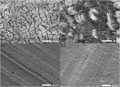 Fig. 3. Microscopy views at 1700× were obtained for R1, R3 and R4. 1900× magnification was used for R2. The images obtained using 2.0 kV, under LED and the height of the specimen stage, WD, differed for each ramp, R1) 19.8 mm, R2) 25.1 mm, R3) 25.1 mm and R4) 24.7 mm.The low magnification SEM images of coating surface morphology formed in processes R1, R2, R3, and R4 are presented in Fig. 3, Fig. 4. The surface of a coating formed in process R1 exhibits numerous cracks and crevices. A powdery appearance and a poor adhesion of this coating indicate that it was burned due to local spikes of the current density. The appearance of whitish spots in the image of a coating built in process R2 also indicates it burning in localized areas. Images of coatings formed in processes R3 and R4 show that they are relatively uniform and smooth. Undulations seen in these coatings along the grain boundary are relatively small.
Each SEM image in Fig. 4 display five sampling sites labeled 1–5 where the EDS analysis was performed. Due to similarity, the EDS plots are reported in Fig. 4 only for sites 1 and 2. Plots in Fig. 5, Fig. 6, Fig. 7, Fig. 8 demonstrate the effect of anodizing regimes R1, R2, R3, and R4 on the content of aluminum, oxygen, sulfur, and zinc in an oxide coating.
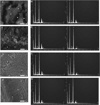 Fig. 4. Microscopy views and EDS results at 19,000× were obtained using 5.0 kV, under LED and the height of the specimen stage, WD, was 10.0 mm. SEM images and EDS plots for sites 1 (left) and 2 (right), respectively, are presented in a, b) R1; c, d) R2; e, f) R3; and g, h) R4.
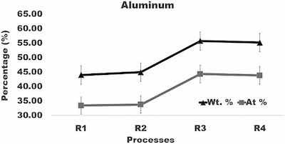 Fig. 5. Graph of the amount of aluminum in surface layer formed after anodizing of aluminum using varying current density processes.
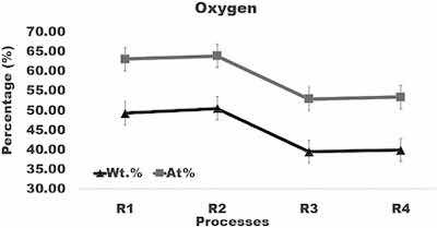 Fig. 6. Graph of the amount of oxygen in surface layer formed after anodizing of aluminum using varying current density processes.
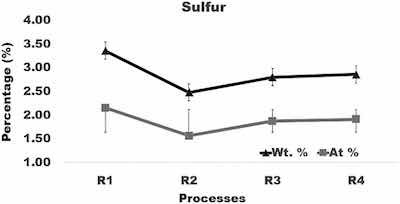 Fig. 7. Graph of the amount of sulfur in surface layer formed after anodizing of aluminum using varying current density processes.
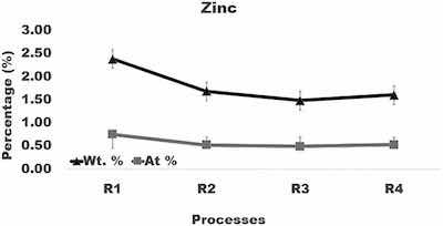 Fig. 8. Graph of the amount of zinc in surface layer formed after anodizing of aluminum using varying current density processes.
The highest aluminum concentration of about 55 wt% was found in coatings formed in processes R3 and R4. It is greater by about 10 wt% than the aluminum content in coatings built in processes R1 and R2. Comparison of the aluminum content in coatings formed in processes R1, R2, R3, and R4 (Fig. 5) demonstrates that a difference between concentrations of aluminum in coatings created by different anodizing regimes exceeds variation of the aluminum level within a coating formed under the same anodizing conditions. The lowest oxygen content of about 39 wt%, was found in coatings formed in process R3 and R4. It is smaller by about 10 wt% than the oxygen concentration in coatings built in processes R1 and R2. Comparison of oxygen concentration in coatings formed in processes R1, R2, R3, and R4 (Fig. 6) shows clearly that a difference between the oxygen level in coatings created by different anodizing regimes exceeds variation of the oxygen level within a coating built under the same anodizing conditions.
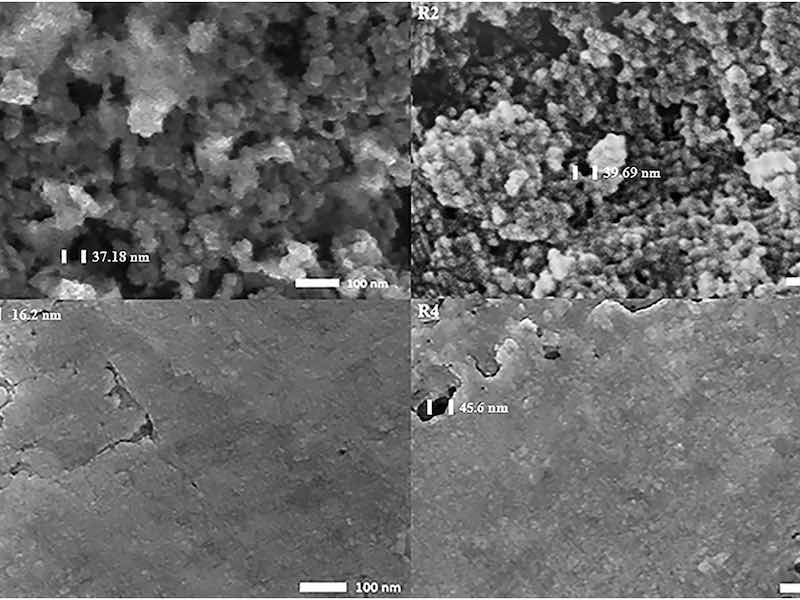
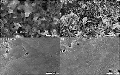 Fig. 9. Microscopy views at 100,000× were obtained using 10.0 kV, under LED and the height of the specimen stage, WD, was 10.0 mm of processes R1, R2, R3, and R4. Pore diameter size and locations are identified for reference.Coatings with the atomic Al/O ratio of 0.53 were formed in R1 and R2 processes, whereas this ratio was 0.83 in coatings built in R3 and R4 processes. The former is smaller than the Al/O stoichiometric ratio of 0.67 in Al2O3 oxide, whereas the latter is greater. A higher percentage of aluminum and a lower percentage of oxygen in coatings created in processes R3 and R4 made the coating surface smooth and solid-like as it seen in SEM images in Fig. 3, Fig. 4. In contrast, a lower percentage of aluminum and a higher level of oxygen infused into coatings formed in processes R1 and R2 caused them to burn and exhibit a powdery appearance as can be seen in SEM images in Fig. 3, Fig. 4.
Sulfur was adsorbed into the oxide layer with SO4 ions penetrating from the electrolyte. The average sulfur level in coatings formed in processes R2, R3, and R4 (Fig. 7) is smaller by about 0.5 wt% than in coatings built in process R1. Zinc diffused into an oxide layer from the alloy matrix. Compared to R1, the average content of zinc in samples anodized in processes R2, R3, and R4 is smaller by about 0.6 wt%. However, comparison of the sulfur and zinc levels in coatings formed in processes R1, R2, R3, and R4 (Fig. 7, Fig. 8) shows that their differences fall within variations of the sulfur and zinc concentrations from location to location in a coating built under the same anodizing conditions.
High-magnification SEM images of the surface of anodic films developed in processes R1-R4 are presented in Fig. 9. Values of the pore diameter, interpore distance and pore density are given in Table 5. Pore density was calculated using Eq. (4) [35]:
N = [2 x 10⁶] / [√3 (Dint2)] (4)
where N is the number of pores per unit area in μm2 and Dint is the interpore distance in nm. As can be seen in Table 5, the observed dependence of the interpore distance and pore density on the applied initial voltage is consistent with Eq. (5) [36] for the porosity of anodic aluminum oxides formed in sulfuric acid electrolyte:
Dint = 12.1 + 1.99•U for 3 ≤ U ≤ 18 (5)
where U is the applied voltage in V.
Table 5. Pore diameter, interpore distance, and pore density in coatings formed in anodizing processes R1, R2, R3, and R4.
| Processes | Pore diameter (nm) | Interpore distance (nm) | Pore density (1/μm2) |
| R1 | 68.8 ± 29.8 | 38.8 ± 5.2 | 815.5 ± 251.2 |
| R2 | 62.8 ± 30.8 | 30.8 ± 5.7 | 1574.5 ± 855.5 |
| R3 | 24.8 ± 7.6 | 21.8 ± 4.1 | 2515.1 ± 907.4 |
| R4 | 43.4 ± 8.3 | 17.2 ± 3.8 | 4506.8 ± 1877.4 |
High-resolution SEM images (100,000×) in Fig. 9 demonstrate that processes R3 and R4 formed more intact coatings with fewer voids and crevices. They are not visible in SEM images presented in Fig. 3, Fig. 4 which were taken at a lower magnification. Whereas the depth of crevices in coatings built in R3 and R4 processes is 0.01–0.02 μm, crevices in coatings formed in R1 and R2 processes are 0.1–0.2 μm deep. Due to a smaller size of pores, coatings developed by processes R3 and R4 demonstrated higher hardness and resistance to abrasion. For R3 and R4, small pores can be seen in areas of delaminated coating in the upper left of Fig. 9, whereas the majority of the coating has been fused together into a continuous film elsewhere. R1 and R2 exhibit a patchy coating which makes the pore structure visible. However, it did not increase their corrosion resistance that is mainly controlled by the ability to inhibit the penetration of corrosion elements to the substrate metal.
3.6. XRD patterns of anodized samples
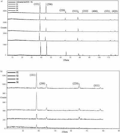 Fig. 10. A) XRD measurements on samples of the untreated alloy AA7075-T6 and alloy samples anodized in processes R1, R2, R3, R4 collected at incident angles 50. B) XRD measurements on samples anodized in processes R1, R2, R3, R4 collected at incident angles 20 using grazing technique.Results of XRD measurements on samples anodized in processes R1, R2, R3, R4 and, for comparison, on samples of the untreated alloy AA7075-T6 are shown in Fig. 10(a–b). Compared to the XRD data collected at an incident angle of 50 (regular regime), the contribution of signals from the substrate in the grazing XRD collected at an incident angle of 20 was reduced while the contribution of signals from the coating was enhanced. Grazing XRD was taken to provide more information about characteristics of the coating, with trying to reduce the effects of the base material. According to the instrument peak profiles, eight peaks in XRD patterns collected at an incident angle of 50 and four peaks collected at an incident angle of 20 corresponded to the aluminum face-centered-cubic (fcc) crystal structure. However, specific diffraction peaks of aluminum oxides were not observed in both types of diffraction patterns collected on anodized samples. It indicates that amorphous aluminum oxides formed in the coating.
Compared to the untreated alloy, anodization changed the position and width of peaks in diffraction patterns. The lattice constant of the fcc structure of samples reported in Fig. 11(a) was computed for both types of XRD measurements from Eq. (6) [37].
dhkl = a / [√(h2 + k2 + l2)] (6)
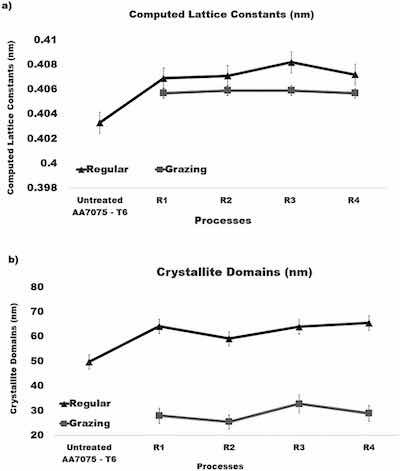 Fig. 11. A) Computed lattice constants of the FCC structure of crystallites. B) Computed sizes of crystalline domains.where dhkl is the distance between the adjacent lattice planes in the fcc structure for the peak Bragg angle in nm, a is the lattice constant/parameter in nm, and hkl are the Miller indices for the lattice planes. Plots in Fig. 11 (a) show that lattice constants of crystallites in anodized samples calculated from both types of XRD measurements are consistent and slightly larger than that of the untreated alloy.
The Scherrer equation, Eq. (7) [37], was taken to compute the size of coherently scattering crystalline domains from the peak width
L = Kλ / βhklcos(θhkl) (7)
where L is the mean size of the crystalline domains in nm, K = 0.9 is the shape factor, λ = 0.15406 nm is the wavelength of the CuKα radiation, θhkl is the peak Bragg angle in radians, βhkl is the corrected value of the full width at half-maximum (FWHM) of the peak in radians, and hkl are the Miller indices of the crystallographic planes. The measured broadening, Eq. (8) [37], of a peak was corrected by the data on the instrumental peak broadening as
βhkl = (β2hkl - β2ints, hkl) (8)
where βm,hkl(rad) is the measured FWHM, and βinst,hkl (rad) is the instrumental FWHM. Estimated values of βinst,hkl at the scanning regime utilized in the XRD measurements were kindly provided by Dr. Mirko Schoenitz (New Jersey Institute of Technology, New Jersey). They were calculated from data on the peaks in diffraction patterns of annealed spheroidal aluminum powders.
Plots in Fig. 11(b) present data on the crystalline domain sizes for both types of XRD measurements. Results of these calculations were averaged over all peaks identified in the diffraction pattern and then averaged over three samples. As can be seen from Fig. 11 (b), the size of crystalline domains in anodized samples computed from measurements at an incident angle of 50 (regular regime) is larger than in the untreated alloy. However, the size of crystalline domains in anodized samples found from data on the grazing XRD appear to be nearly twice smaller. This outcome is related to the fact that the contribution of signals from the substrate is reduced while the contribution of signals from the coating is enhanced in the grazing XRD measurements. It is also noticeable in Fig. 11 that variations of the anodization regime do not seem to have an impact on the lattice constants and the size of crystalline domains.
3.7. Electric charge transferred during anodization
The amount of voltage applied in anodization controls the electric current and ultimately the coating formation. Table 6 lists the anodizing current specified by Table 2 and presents average data on measured initial and final voltage for each ramping step of processes R1, R2, R3, and R4. The difference between the charge transferred during a ramping stage and the value listed in Table 2 is lying within several percentages as the accuracy of maintaining the constant anodizing current was about 1%. The voltage measurements presented in Table 6 were used to compute the work required to transfer the electric charge specified in Table 2. The work performed in each run is equal to the product of the applied voltage and the electric charge. Results are summarized in Table 7.
Table 6. Data on the applied anodizing current specified in Table 2 and the measured initial and final voltage for each ramping step of processes R1, R2, R3, and R4. The presented voltage values were averaged over three runs.
| Minutes | Amps | Initial voltage (V) | Final voltage (V) |
| Process R1 | |||
| 30 | 22 | 12.3 ± 0.2 | 13.9 ± 0.3 |
| Process R2 | |||
| 5.00 | 13 | 7.5 ± 0.17 | 10.7 ± 0.12 |
| 5.00 | 17 | 11.8 ± 0.22 | 12.1 ± 0.21 |
| 20.00 | 25 | 12.6 ± 0.26 | 14.2 ± 0.17 |
| Process R3 | |||
| 2.50 | 8 | 4.6 ± 0.12 | 6 ± 0.21 |
| 2.50 | 13 | 8.5 ± 0.12 | 8.8 ± 0.2 |
| 2.50 | 17 | 10.6 ± 0.17 | 10.9 ± 0.12 |
| 2.50 | 21 | 11.7 ± 0.16 | 11.9 ± 0.13 |
| 20.00 | 25 | 12.1 ± 0.3 | 13.9 ± 0.18 |
| Process R4 | |||
| 1.25 | 6 | 3.7 ± 0.1 | 4.9 ± 0.16 |
| 1.25 | 8 | 5.7 ± 0.28 | 6.5 ± 0.12 |
| 1.25 | 10 | 7.1 ± 0.16 | 7.6 ± 0.16 |
| 1.25 | 13 | 8.2 ± 0.25 | 8.7 ± 0.12 |
| 1.25 | 17 | 9.4 ± 0.16 | 9.6 ± 0.21 |
| 1.25 | 19 | 10.3 ± 0.24 | 10.7 ± 0.12 |
| 1.25 | 21 | 10.9 ± 0.12 | 11.2 ± 0.1 |
| 1.25 | 23 | 11.4 ± 0.17 | 12.1 ± 0.17 |
| 20.00 | 25 | 12.7 ± 0.17 | 13.1 ± 0.17 |
Table 7. Total work (kJ) required to transfer the electric charge specified in Table 2 during anodization, the coating formation rate (μm/min), and the electric charge transferred per layer thickness of (C/μm). Data for the total work averaged over three 30-min runs of anodizing processes R1, R2, R3, and R4.
| Processes | Work (kJ) | Rate of coating formation (μm/min) | Charge per layer thickness (C/μm) |
| R1 | 13;511 ± 115 | 0.34 | 3412 |
| R2 | 16;358 ± 461 | 0.37 | 3491 |
| R3 | 17;014 ± 401 | 0.43 | 3138 |
| R4 | 16;506 ± 269 | 0.44 | 3158 |
The amount of voltage applied to initiate the processes decreased with increasing the number of steps from R1 to R4 (Table 6). A larger work was performed to build an oxide layer on the metal surface in processes R3 and R4 (Table 7). Compared to processes R1 and R2, processes R3 and R4 required a shorter period of applying an elevated voltage that suppressed the appearance of burning and processing defects in formed oxide layers. Processes R3 and R4 also provided a higher rate of the coating growth while requiring a smaller electric charge per one micrometer of the coating thickness (Table 7). As can be seen in Table 6, Table 7, basic characteristics of processes R3 and R4 are similar. Both demonstrated the layer growth rate faster by 23.4% and 25.6%, respectively, than conventional process R1. It indicates that ramping the anodizing current density and consequently the applying voltage allows for more efficient coating formation later in the process. Interestingly, improvement of the mechanical properties of coatings formed in processes R2, R3, and R4 compared to R1 strongly correlates with increasing the amount of work implemented to form the oxide layer (Table 7).
4. Conclusion
This study successfully demonstrated the overall advantages of multistep anodization of AA 7075-T6. Four anodizing regimes in a sulfuric acid bath were considered: a conventional R1 with a constant applied current and R2, R3, R4 with ramping of an applied current in two, four, and eight steps, respectively. Since oxides grew more slowly in initial lower-voltage steps of R3 and R4, the electrical resistance of the oxidized layer during this period was lower, which allowed heat to dissipate more readily and thereby suppressed formation of burns and defects. Compared to R1, multistep current ramping in R3 and R4 increased the overall growth rate of oxides by 23.4% and 25.6%, respectively and reduced by 8.4% the amount of a transferred electric charge per micrometer of the layer thickness. Like other conventional methods, process R1 was accompanied with spikes and burns at the beginning and did not provide a sufficient current at the end.
Processes R1 and R2 formed coatings with the atomic Al/O ratio of 0.53 smaller than 0.67 for oxide Al2O3, whereas R3 and R4 created coatings with the Al/O ratio of 0.83. A higher level of oxygen infused into coatings built in R1 and R2 caused them to burn and exhibit a powdery appearance, whereas processes R3 and R4 formed coatings with a smooth solid-like surface. Coatings created in processes R3 and R4 have substantially smaller number of crevices and their depth was about 0.01–0.02 μm, whereas crevices in coatings formed in R1 and R2 were 0.1–0.2 μm deep. The pore size in the coatings formed in processes R1 and R2 was about 94% and 87% larger than in the coatings formed in processes R3, respectively. Compared to R1, process R4 created coatings that were 74.0% more resistant to abrasion, 14.6% harder and 25.4% thicker. As no specialized equipment is required, the presented multistep anodization is well suited for large-scale manufacturing.
Peter Totaro, Ph.D., is the Vice President of Operations and head of Engineering at Aerotech Processing Solutions in Paterson, New Jersey. Boris Khusida, Ph.D., is Professor of Chemical and Materials Engineering at the New Jersey Institute of Technology in Newark, NJ.
Credit authorship contribution statement: Peter Totaro: Conceptualization, Methodology, Experiments, Data curation and analysis, Writing – original draft, review & editing. Boris Khusid: Supervision, Conceptualization, Data curation and analysis, Writing – review & editing.
Declaration of competing interest: The authors declare that they have no known competing financial interests or personal relationships that could have appeared to influence the work reported in this paper.
Acknowledgements: The authors are thankful to Dr. Mirko Schoenitz (New Jersey Institute of Technology, New Jersey) for providing data on the instrumental peak broadening in XRD measurements and Qian Lei (New Jersey Institute of Technology, New Jersey) for providing guidelines on image processing and analysis with ImageJ. This research did not receive any specific grant from funding agencies in the public, commercial, or not- for-profit sectors.
References
[1] I. Mohammadi, S. Ahmadi, A. Afshar; Effect of pulse current parameters on the mechanical and corrosion properties of anodized nanoporous aluminum coatings; Mater. Chem. Phys., 183 (2016), pp. 490-498, 10.1016/j.matchemphys.2016.09.006
[2] E. Ghali Corrosion Resistance of Aluminum and Magnesium Alloys: Understanding, Performance, and Testing (first ed.), Wiley, New Jersey (2010)
[3] J.M. Runge The Metallurgy of Anodizing Aluminum: Connecting Science to Practice Springer International Publishing AG (2018)
[4] L. Song-mei, Z. Hong-rui, L. Jian-hua; Corrosion behavior of aluminum alloy 2024-T3 by 8-hydroxy- quinoline and its derivative in 3.5% chloride solution; Trans. Nonferrous Metals Soc. China, 17 (2) (2007), pp. 318-325, 10.1016/S1003-6326(07)60092-2
[5] A. Venugopal, R. Panda, S. Manwatkar, K. Sreekumar, R. Krishna, G. Sundararajan; Effect of micro arc oxidation treatment on localized corrosion behavior of AA7075 aluminum alloy in 3.5% NaCl solution; Trans. Nonferrous Metals Soc. China, 22 (3) (2012), pp. 700-710, 10.1016/S1003-6326(11)61234-X
[6] L. Bouchama, N. Azzouz, N. Boukmouche, J.P. Chopart, A.L. Daltin, Y. Bouznit; Enhancing aluminum corrosion resistance by two-step anodizing process; Surf. Coat. Technol., 235 (2013), pp. 676-684, 10.1016/j.surfcoat.2013.08.046
[7] J. Son, H. Nakano, S. Oue, S. Kobayashi, H. Fukashima, Z. Hortia; Effect of equal-channel angular pressing on pitting corrosion resistance of anodized aluminum-copper alloy; Trans. Nonferrous Metals Soc. China, 19 (4) (2009), pp. 904-908, 10.1016/S1003-6326(08)60374-X
[8] A. Bozza, R. Giovanardi, T. Manfredini, P. Mattiolo; Pulsed current effect on hard anodizing process of 7075-T6 aluminum alloy; Surf. Coat. Technol., 270 (2015), pp. 139-144, 10.1016/j.surfcoat.2015.03.010
[9] M.E. Fine; Precipitation hardening of aluminum alloys; Metall. Trans. A., 6 (1975), pp. 625-630, 10.1007/BF02672283
[10] P.G. Sheasby, R. Pinner; The Surface Treatment and Finishing of Aluminum and Its Alloys; (6th ed.), Finishing Publications Ltd. and ASM International, Materials Park, Ohio (2001)
[11] W.E. Cooke; Factors affecting loss of brightness and image clarity during anodizing of bright trim aluminum alloys in sulfuric acid electrolyte; Plating, 49 (1962), pp. 1157-1165
[12] C.K. Chung, W.T. Chang, M.W. Liao, H.C. Chang; Effect of pulse voltage and aluminum purity on the characteristics of anodic aluminum oxide using hybrid pulse anodization at room temperature; Thin Solid Films, 519 (15) (2011), pp. 4754-4758, 10.1016/j.tsf.2011.01.029
[13] M. Roshani, A. Sabour Rouhaghdam, M. Aliofkhazraei, A. Heydari Astaraee; Optimization of mechanical properties for pulsed anodizing of aluminum; Surf. Coat. Technol., 310 (2017), pp. 17-24, 10.1016/j.surfcoat.2016.12.046
[14] M. Bononi, R. Giovanardi, A. Bozza, P. Mattioli; Pulsed Current Effect on Hard; (2016), 10.1016/j.surfcoat.2016.01.056
[15] L. Iglesias-Rubianes, S.J. Garcia-Vergara, P. Skeldon, G.E. Thompson, J. Ferguson, M. Beneke; Cyclic oxidation process during anodizing of Al–Cu alloys; Electrochim. Acta, 52 (2007), pp. 7148-7157, 10.1016/j.electacta.2007.05.052
[16] X. Zhou, G.E. Thompson, H. Habazaki, K. Shimizu, P. Skeldon, G.C. Wood; Copper enrichment in Al–Cu alloys due to electropolishing and anodic oxidation; Thin Solid Films, 293 (1997), pp. 327-332, 10.1016/S0040-6090(96)09117-1
[17] M. Saenz de Miera, M. Curioni, P. Skeldon, G.E. Thompson; Preferential anodic oxidation of second-phase constituents during anodizing of AA2024-T3 and AA7075-T6 alloys; Surf. Interface Anal., 42 (2010), pp. 241-246, 10.1002/sia.3191
[18] A. Pakes, G.E. Thompson, P. Skeldon, P.C. Morgan; Development of porous anodic films on 2014-T4 aluminium alloy in tetraborate electrolyte, Corros; Sci., 45 (2003), pp. 1275-1287, 10.1016/S0010-938X(02)00216-0
[19] X.F. Zhu, D.D. Li, Y. Song, Y.H. Xiao; The study of oxygen bubbles of anodic alumina based on high purity aluminum; Mater. Lett., 59 (2005), pp. 3160-3163, 10.1016/j.matlet.2005.05.038
[20] H. Habazaki, H. Konno, K. Shimizu, S. Nagata, P. Skeldon, G.E. Thompson; Incorporation of transition metal ions and oxygen generation during anodizing of aluminium alloys; Corros. Sci., 46 (2004), pp. 2041-2053, 10.1016/j.corsci.2003.10.027
[21] J.R. Davis; Alloying: Understanding the Basics, Aluminum and Its Alloys; (first edition), ASM International, Ohio (2001)
[22] J.W. Diggle, T.C. Downie, C.W. Goulding; Anodic oxide films on aluminum; Chem. Rev., 69 3 (1969), pp. 365-405, 10.1021/cr60259a005
[23] F. Schaedel; The leading edge guide to top quality anodizing using the complete spectrum approach with a universal type I-II-III (123) mixed electrolyte; Prod. Finish., 76 9 (2012), pp. 1-13; https://www.pfonline.com/articles/electrodeposition-of-ni-fe-mo-w-alloys---15th-quarterly-report
[24] P. Michaf, A. Vagaskâ, M. Gombâr, A. Hošovský, J. Kmec; Monitoring of influence of significant parameters during anodizing of aluminum; IEEE 12th International Symposium on Applied Machine Intelligence and Informatics (SAMI), Herl'any (2014), pp. 49-54; https://ieeexplore.ieee.org/document/6822447
[25] C.K. Chung, M.W. Liao, H.C. Chang, C.T. Lee; Effects of temperature and voltage mode on nanoporous anodic aluminum oxide films by one-step anodization; Thin Solid Films, 520 5 (2011), pp. 1554-1558, 10.1016/j.tsf.2011.08.053
[26] J.M. Runge, T. Hossain; Interfacial phenomena in 7000 series alloys and their impact on the anodic oxide; Mater. Today Proc., 2 10 (2015), pp. 5055-5062, 10.1016/j.matpr.2015.10.096
[27] Z. Ding; Mechanistic study of thin film sulfuric acid anodizing rate difference between Al2024 T3 and Al6061 T6; Surf. Coat. Technol., 357 (2019), pp. 280-288, 10.1016/j.surfcoat.2018.09.083
[28] H.H. Shih, S.L. Tzou; Study of anodic oxidation of aluminum in mixed acid using a pulsed current; Surf. Coat. Technol., 124 (2000), pp. 278-285, 10.1016/S0257-8972(99)00646-5
[29] X. Zhao, G. Wei, X. Meng, A. Zhang; High performance alumina films prepared by direct current plus pulse anodization; Surf. Eng., 30 (2014), pp. 455-459, 10.1179/1743294414Y.0000000258
[30] L.E. Fratila-Apachitei, J. Duszczyk, L. Katgerman; A1–Si–(Cu) anodic oxide layers formed in H2SO4 at low temperature using different current waveforms; Surf. Coat. Technol., 165 (2003), pp. 232-240, 10.1016/S0257-8972(02)00733-8
[31] W. Wu, J.S. Yuan, S.H. Kang, A.S. Oates; Electromigration subjected to Joule heating under pulsed DC stress; Solid State Electron., 45 (2001), pp. 2051-2056, 10.1016/S0038-1101(01)00185-X
[32] ASM Handbook Volume 2: Properties and Selection: Nonferrous Alloys and Special-Purpose Materials, ASM International, Novelty, Ohio (1990), pp. 62-122
[33] ImageJ; Image Processing and Analysis; https://imagej.nih.gov/ij/, Accessed 30th May 2021
[34] M. Curioni, P. Skeldon, G.E. Thompson, J. Ferguson; Graded anodic film morphologies for sustainable exploitation of aluminum alloys; Adv. Mater. Res., 38 (2008), pp. 48-55, 10.4028/www.scientific.net/AMR.38.48
[35] S. Zaidi, M. Butt, F. Bashir; A comparative study of the anodic alumina film thickness measured via SEM and evaluated using Faraday’s Law; Mater. Res. Express, 6 (4) (2019), p. 46404; https://orcid.org/0000-0002-4214-9335
[36] W. Lee, S. Park; Porous anodic aluminum oxide: anodization and templated synthesis of functional nanostructures; Chem. Rev., 114 (15) (2014), pp. 7487-7556, 10.1021/cr500002z
[37] C. Suranarayana, M.G. Norton; X-ray Diffraction: A Practical Approach; Springer, New York (1998)