The following patents related to the finishing and coating industry were granted by the U.S. Patent and Trademark office.
Electroplate Laminated Structure And Methods Of Fabricating The Same
Inventors: Piascik; James; (Randolph, NJ); Wang; David; (Morristown, NJ); Sklar; Glenn; (Randolph, NJ); Mintzer, III; Joseph W.; (Pheonix, AZ); Honeywell International Inc.
Abstract: Corrosion-resistant laminated structures and methods of fabricating laminated structures are disclosed. A method of fabricating a laminated structure includes: providing an object in an electroplating solution; forming a first layer on the object by applying a first electric current, the first electric current being associated with a first current density; and forming a second layer on the first layer by applying a second electric current, the second electric current being associated with a second current density. Each of the first layer and the second layer includes, at least in part, phosphorus. The first current density and the second current density are different.
https://pdfaiw.uspto.gov/.aiw?PageNum=0&docid=20220186394
Method And Apparatus For Monitoring Edge Bevel Removal Area In Semiconductor Apparatus And Electroplating System
Inventors: Wu; Chao-Tung; (Taichung City, Tw); Yu; Kuo-Chung; (Tainan City, Tw); Hu; Chung-Hao; (Hsinchu City, Tw); Weng; Sheng-Ping; (Tainan City, Tw); Taiwan Semiconductor Manufacturing Company LTD.
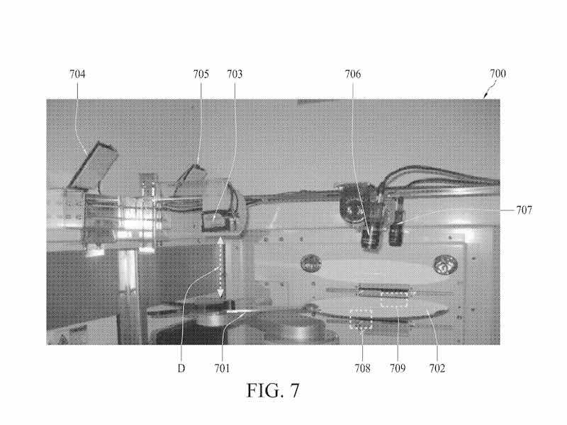
Abstract: A semiconductor apparatus includes a transfer chamber, an annealing station, a robot arm, an edge detector and a trigger device. The transfer chamber is configured to interface with an electroplating apparatus. The robot arm is arranged to transfer a wafer from the transfer chamber to the annealing station. The edge detector, disposed over a predetermined location between the transfer chamber and the annealing station, comprises a first charge-coupled device (CCD) sensor and a second CCD sensor. When the robot arm is carrying the wafer to pass through the predetermined location, the first CCD sensor and the second CCD sensor are located over a first portion and a second portion of the edge bevel removal area respectively, and the trigger device is configured to activate the first CCD sensor and the second CCD sensor to capture an image of the first portion and an image of the second portion respectively.
https://pdfaiw.uspto.gov/.aiw?Docid=20220187216
Protection Of Seed Layers During Electrodeposition Of Metals In Semiconductor Device Manufacturing
Inventors: Zhu; Huanfeng; (West Linn, OR); Reid; Jonathan David; (Sherwood, OR); Zhou; Jian; (Portland, OR); Majid; Tariq; (West Linn, OR); Lam Research Corporation, Fremont, CA, US.
Abstract: A protective layer is formed over a copper seed layer on a semiconductor substrate prior to electroplating. The protective layer is capable of protecting the copper seed layer from oxidation and from dissolution in an electrolyte during initial phases of electroplating. The protective layer, in some embodiments, prevents the copper seed layer from contacting atmosphere, and from being oxidized by atmospheric oxygen and/or moisture. The protective layer contains a metal that is less noble than copper (e.g., cobalt), where the metal can be in an oxidized form that is readily soluble in a plating liquid. In one embodiment a protective cobalt layer is formed by depositing cobalt metal by chemical vapor deposition over copper seed layer without exposing the copper seed layer to atmosphere, followed by subsequent oxidation of cobalt to cobalt oxide that occurs after the substrate is exposed to atmosphere. The resulting protective layer is dissolved during electroplating.
https://pdfaiw.uspto.gov/.aiw?Docid=20220208604
Photoresist Resolution Capabilities By Copper Electroplating Anisotropically
Inventors: Lifschitz Arribio; Alejo M.; (Waltham, MA); Zielinski; Alexander; (Charlton, MA); Hammoodi; Samer; (Worcester, MA); Lachowski; Joseph F.; (Sutton, MA); Gallagher; Michael K.; (Hopkinton, MA); Williamson; Curtis; (Cambridge, MA); Prange; Jonathan D.; (Lincoln, MA). Rohm and Haas Electronic Materials, Marlborough; MA
Abstract: Features of substrates are copper electroplated by a method which involves copper electroplating selectively deposited seed layers or seed layers of photoresist defined features with a copper electroplating composition containing select suppressor compounds and select leveler compounds which enable anisotropic plating. Optionally, the seed layers can be treated with an aqueous solution of sulfur containing accelerators prior to copper electroplating.
Additive For Electroplating Solutions, Electroplating Solution, Electroplating Method And Novel Compound
Inventors: Takahashi; Takuya; (Tokyo, Jp) ; Ishiwata; Shinya; (Tokyo, Jp) ; Hatsukade; Tomoko; (Tokyo, Jp); Adeka Corporation, Tokyo
Abstract: Provided is an additive for an electroplating solution, including a compound represented by the following general formula (1): ##STR00001## where R.sup.1 to R.sup.3 each independently represent a group represented by the following general formula (2), A.sup.1 represents an alkanediyl group having 2 to 4 carbon atoms, and "n" represents 0 or 1: ##STR00002## where R.sup.4 and R.sup.5 each independently represent a hydrogen atom or an alkyl group having 1 to 4 carbon atoms, A.sup.2 and A.sup.3 each independently represent an alkanediyl group having 2 to 4 carbon atoms, "m" represents an integer of from 1 to 4, and * represents a bonding site.
https://pdfaiw.uspto.gov/.aiw?Docid=20220220065
Anodizing Device
Inventors: Chang; Hyunsoo; (Asan-si Chungcheongnam-do, KR); Mando Corporation, Pyeongtaek-siGyeonggi-do, KR.
Abstract: Provided is a anodizing apparatus, including: a base configured to support a target product including a first bore that requires an anodizing surface treatment and a second bore that is connected to the first bore and excluded from the anodizing surface treatment; a working part configured to perform the anodizing surface treatment on the first bore; and a cover part configured to cover an outer surface of the target product, wherein the working part includes at least one electrode bar configured to access and enter the first bore, and a plurality of spray nozzles provided integrally with each of the at least one electrode bar and configured to selectively supply one of a degreasing solution, an electrolyte, and a cleaning solution to the first bore.


