


Zircon-based thin film pretreatment is increasingly applied in automotive industry, because of several benefits compared to the phosphating process.
 Tobias LuxBut after rolling out, several impacts on the electrophoretic coating process were observed, like film thickness spread on various substrate materials, dependence on drying status, or worsened appearance. To gain a better understanding of the interaction between pretreatment and electrocoating, the effect of several electrocoating process factors on the two main deposition parameters, coulombic yield and wet film resistance, is investigated. The experimental setup with gradually increasing electrical charge reveals a third main deposition parameter, the charge threshold. At the beginning of the deposition process, electrical charge is consumed but only a minimal amount of coating is deposited. Furthermore, this setup allows for a more robust definition of coulombic yield. The magnitude of the charge threshold, that is correlated to the induction time, depends on pretreatment and substrate material, whereas the coulombic yield is hardly affected by these factors. The influence of pretreatment on wet film resistance and charge threshold is explained by the different occurrences of hydrogen gas bubbles on the panel substrate and in the coating. The distribution of non-conductive hydrogen bubbles is assumed to restrain the mobility of the hydroxide ions in the wet film and influence its electrical resistance.
1. Introduction
Painting of a car body requires a sequence of preparation processes. The body in white first undergoes several cleaning and rinsing steps, followed by a pretreatment process, followed by several more rinsing steps before proceeding to the electrocoating (“EC”) process. The aim of the pretreatment (“PT”) is to provide proper adhesion of the subsequent cathodic electrodeposition paint and to enhance the corrosion resistance of the paint system. Phosphating, typically involving a tri-cation phosphate of zinc, nickel and manganese, is the most widely used PT process in the automotive industry. Despite its excellent properties, efforts are underway to replace this process with a more environmentally friendly and less energy-consuming pretreatment method. Zircon-based thin film PT technologies are now increasingly applied, offering several advantages compared to phosphating. The Thin Film Pretreatment (“TFPT”) process typically operates at room temperature, allows for high or even 100% Aluminum content of the car body, produces less wastewater and does not require periodic bath cleaning with strong acids.
Following the initial implementation of TFPT processes in manufacturing plants, detrimental effects on the electrodeposition process became apparent. Compared to phosphated car bodies, the appearance of the electrocoat deteriorates and the coating thickness exhibits greater variability across different substrate materials. The dependence of film thickness on the substrate type after phosphating is minimal. In contrast, after TFPT, the electrocoat film thickness e.g. on Aluminum in relation to galvanized steel or between bare steel and (electro-) galvanized steel, might differ by several micrometers, potentially leading to visible defects and requiring rework. These effects are more pronounced instantly after pretreatment (wet in wet) than on dried surfaces, potentially resulting in visible structures on partly dried car bodies. Local flow velocity differences in the TFPT bath can cause film thickness differences of the electrocoat and induce visible defects. Many car manufacturers use a simulation tool to predict the thickness of the deposited electrocoat of the car body. The simulation is used to optimize the part geometry for the electrocoating process. The algorithms of these tools must be adapted to the different deposition conditions on phosphated and thin film pretreated substrates.
The aforementioned film thickness spread, the deteriorated appearance, and the insufficient precision of the simulation tool necessitate a deeper understanding of the mechanisms of the electrocoat deposition process and its relationship with the substrate’s surface condition pretreatment. To address this, a series of coating experiments was carried out, in which pretreatment methods, substrate material, and other process parameters were varied. During these experiments, an effect was observed that, to our knowledge, has not yet been described. At the beginning of the coating process, despite continuous current flow, no layer deposition measurable with a milligram balance can be detected. Only after a certain charge limit is exceeded is a linear increase in the deposited mass with the flowed electrical charge recorded. This effect is referred to as "charge threshold" in this publication. In contrast to the previous practical determination of the coulombic yield from a defined single experiment, derived from these test series, the slope of the linear mass increase with charge after exceeding the charge threshold is proposed. This definition is independent of various substrate materials and pretreatments. Essential for the uniformity of layer deposition is the development of wet film resistance on different substrates. The clear dependence on pretreatment is investigated in a further series of coating experiments, and the influence of gas bubble distribution is proposed as a co-determining factor. A better understanding of the mechanisms involved could enable the future development of customized PT and EC materials. Improved insight into the deposition mechanisms can also be utilized for a more precise simulation of film thickness on complex-shaped multi-metal car bodies.
1.1. Deposition theory
Cathodic electrodeposition paints used in automotive coating comprise several components, supplied as two main feeding components, binder and pigment paste [1]. Mixed with water they form the EC bath, with a non-volatile ratio of usually about 20%. The main component of the binder is the epoxy resin. The molar mass of the resin polymer chains can range from 1000 to several thousand g/mol [1]. During binder production, the amine groups of the resin react with one or more, typically weak, acids, rendering the resin water-soluble through protonation to ammonium groups. Diluted in water, the resin polymer chains form micelles of an average size ranging from 6 to 140 nm, consisting of 30–150 resin molecules [2]. The protonated amine groups of the polymer chains of the micelles face outwards towards the water interface, attracting the negatively charged counter ions of the acid.
The deposition process is based on the generation of hydroxide ions, which react with the protons of the ammonium groups. Deprotonation of the ammonium groups gradually destabilizes the micelle, which then breaks up upon removal of a certain number of protons, leading to coagulation of the now insoluble binder resin. Through water electrolysis, the necessary hydroxide ions are generated at the cathode and oxonium ions at the anode. The electrolysis process occurs at the interface between the electron conducting substrate and the ion conducting polymer film, respectively before film deposition between substrate and electrolyte. The three main reactions are [3]:
- Reduction (Cathode): 4 H2O + 4 e-Û2 H2 + 4 OH-
- Oxidation (Anode): 6 H2O Û4 H3O++ O2 + 4 e-
- Resin Neutralization: Rx-NH+ + OH-ÛRx-N + H2O
The electrical current for the electrolysis is provided by a rectifier. The electron flux in the external circuit driving the electrode reactions corresponds to an equivalent ion flux at the electrodes and in the electrolyte. Any ion reaching the electrode contributes to the charge flux, whether driven by migration, diffusion or convection. According to Faraday’s laws, reaction rates can be calculated provided the transport numbers of ion species are known [4]. The transport numbers depend on the ion’s mobility and their concentration. It can be assumed that convection will be the main force for micelle movement in the bulk electrolyte, whereas diffusion and migration play a significant role only in the diffusion layer [5].
After deprotonation, the resin molecules begin to build up on the surface. Film growth initially begins by forming islands that subsequently spread laterally. The different structure of the film depending on the pretreatment is shown in Fig. 1. On phosphated substrates, many small islands are formed with visible remnants of hydrogen bubbles. On Oxsilan-pretreated surfaces, the film grows in larger islands without significant remnants of hydrogen bubbles. The dependence of the film structure on the substrate has been described by other authors [6], [7] and will be further discussed in the following chapters. Compared to the uncoated (only pretreated) surface, the resin film induces a substantially higher electrical resistance, thereby concentrating a major part of the current on the uncovered area. The ongoing growth of the resin film gradually reduces the uncovered surface area and increases the equivalent resistance. This can be approximately calculated using the parallel resistances of the uncovered and covered surface areas (see Fig. 2). When the film coverage approaches unity, a sudden, steep rise in the rectifier voltage is necessary to maintain the constant current. The resistance of the bulk electrolyte remains relatively constant throughout the deposition process.
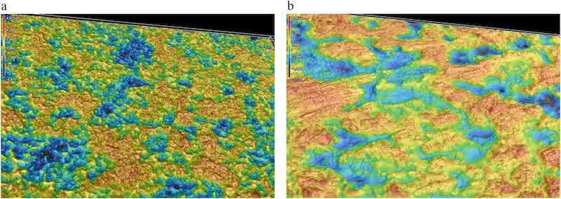
Fig. 1. Initial deposition step of EPIC200RX on MBZE panels: (a) Phosphated; 15.7 mC/cm2; 0.14 mg/cm2; (b) Oxsilan; 47.5 mC/cm2; 0.25 mg/cm2.
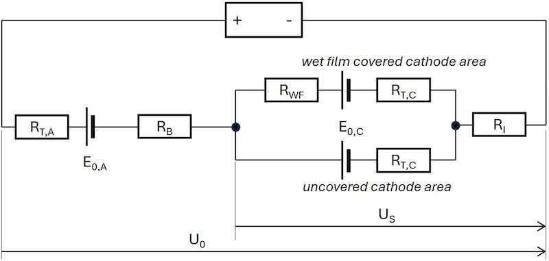
Fig. 2. Simplified equivalent circuit of the deposition setup: Transfer resistance anode RT,A; transfer resistance cathode RT,C; bath resistance RB; wet film resistance RWF; resistance of current measurement transducer RI; rectifier voltage U0; potential sensor voltage US; standard potential anode E0,A; standard potential cathode E0,C.
2. Experimental
2.1. Materials
All panels were standard size 105 × 190 mm, supplied by Chemetall. MBZE panels (electrogalvanized, EG) are according to the VDA standard CR5-EG53/53-E, MBS panels (cold rolled steel, CRS) according to CR5-UC-E, and AA6014 (Aluminum) according to MB standard AL6-OUT-TZ-E (AlMg0,6Si0,6).
The pretreatment of the panels was either pre-deposited by Chemetall with Gardobond 2600 (Tri-cation phosphate) or deposited in a serial production plant with Oxsilan 9835. The phosphated panels are abbreviated in this work by “PH”, the Oxsilan pretreated panels by “OS”.
Two commercially available electrocoat materials were used, BASF CathoGuard 800RE and PPG EPIC 200RX.
2.2. Equipment
All deposition experiments were carried out in laboratory in a 5-liter beaker with an inner diameter of 175 mm. Agitation was ensured by a magnetic stirrer with adjustable rotation speed. The anode was made of a stainless-steel strip of 35 mm width, fixed at 50 mm distance to the cathode.
A rectifier TDK Lambda Genesys 600–5.5 was connected to anode and cathode. A measuring device for 4 current channels was connected inline at the cathode side to the power supply. A measuring device for 4 voltage channels with reference to cathode potential could be used to measure bath potential with a stainless-steel electrode. This electrode was positioned a few millimeters in front of the cathode. The rectifier and the current and voltage measuring device were controlled by a PC program and the values stored on the PC. A simplified equivalent circuit of the deposition setup is shown in Fig. 2. The parallel capacitance of each electrodes charged double layer is omitted in this scheme.
The samples were weighed by a scale Kern PNS 600. The resolution of the scale is 1 mg and repeatability is within + - 1 mg. Film thickness was measured with a Fischer Phascope. The topographic images were taken with a Keyence VK-X200 laser scanning microscope.
2.3. Procedures
For some deposition experiments, the Oxsilan-pretreated panels were kept in ambient climate for a specified period prior to coating to initiate an aging process of the TFPT layer.
The panels were weighed before coating, after coating (prior to baking), and again after baking. To ensure a specific coating area, the panels were masked with adhesive tape, leaving a coating area of 150 cm2on each side. The electrical parameters of the deposition process were maximum voltage and maximum current settings of the rectifier. For the current controlled deposition experiments the rectifier maintained the maximum current as long as the voltage remained below the maximum setting. After reaching the maximum voltage, the current decreased, corresponding to the growing wet film resistance. The deposition experiment was stopped either when a specified value of electrical charge was consumed, or, in some experiments, when the maximum voltage was reached. The rotation speed of the magnetic stirrer was typically 500 rpm, unless otherwise noted. Baking was always done at 175 °C for 15 min (object temperature). From current, voltage, and potential measurements, the consumed charge, the wet film resistance (using the potential value to largely eliminate bath resistance), and the bath resistance were calculated.
The experiments were carried out only once for each parameter set. This limitation must be considered when evaluating the results and the derived quantitative values.
3. Results
Two main parameters govern the EC deposition process. The first parameter is the coulombic yield, which describes the amount of coating deposited relative to the electrical charge consumed. The second parameter is the wet film resistance caused by a given amount of deposited coating. The (locally distributed) wet film resistance controls the current density of each part of the area, relative to the local electric potential of the adjoining electrolyte. This resistance distribution therefore controls the momentary local deposition yield on each part of the surface. Due to the high conductivity of the electrolyte, the electrical potential in neighboring areas of the bath cannot differ significantly. It is necessary to identify and analyze all factors influencing these two main parameters to develop a precise model for the deposition process.
3.1. Coulombic yield
Fig. 3 shows the deposited wet film mass in relation to the charge density. The electrical charge is a parameter that can be easily controlled in laboratory experiments, at least integral for the entire surface of the test part.
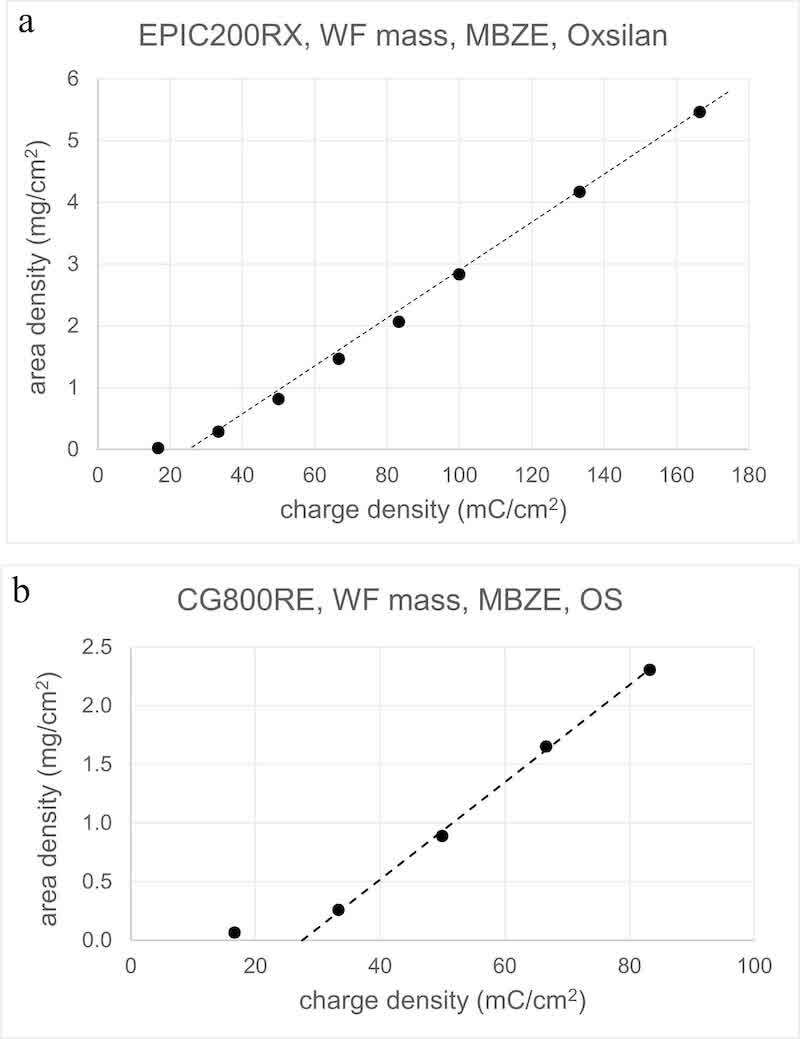
Fig. 3. Wet film mass area density in relation to the density of consumed charge for (a) EPIC200RX and (b) CG800RE on Oxsilan pretreated MBZE panels, both at 32 °C.
Both EC materials exhibit a linear increase of deposited mass in relation to the consumed charge. This linear relationship is well known [6], [8]. A linear increase in the deposited mass with the consumed charge is consistent with the neutralization reaction described in Chapter 1.1, where the average molar mass of the binder resin is linked to the amount of charge from the electrolysis process. In commercial paint materials, however, the influence of other components must also be considered. In the low charge region of both materials, it is evident that an individual charge threshold must be surpassed before significant film growth sets in. The reciprocal slope of the linear region may be taken as the coulombic yield (in C/g) of the deposition process. If the definition of the coulombic yield refers to the linear range of the experimental series instead of a single experiment, factors influencing the charge threshold are eliminated, and a more robust measured value is obtained. The wet film (“WF”) mass is used as the y-axis in these graphs because it is measurable with higher precision than coating thickness and it provides an integral measure of the entire panel, similar to the electrical charge, whereas film thickness is non-uniformly distributed. However, the relationship with other y-axis parameters is similar, as shown, for example, in Fig. 4(a) for the dry film thickness, whose shape is comparable to Fig. 3(a). The linear correlation between wet film mass and dry film (“DF”) thickness is represented in Fig. 4(b). For the calculation of the charge threshold in the following experiments, the linear region had to be defined, and the slope of the regression line calculated. To define the measurement points lying within a sufficiently linear range, the slope between two adjacent points was determined for each case. If the slopes of two adjacent sections differed by only 15%, the first section was defined as the beginning of the linear range. The regression line was then calculated using all measurement points within the linear range. The intersection of the regression line with the x-axis was taken as the value for the charge threshold.
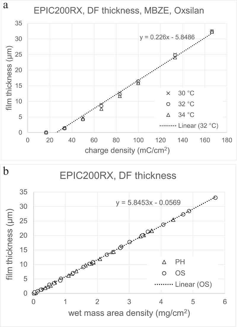
Fig. 4. (a) Film thickness in relation to the density of consumed charge, (b) correlation of dry film thickness to wet film mass area density. Boths graphs are EPIC200RX on MBZE panels.
3.1.1. Temperature
The dependence of the deposited mass on the deposition temperature for both EC materials is presented in Fig. 5. For both materials there is no distinct effect visible, indicating that the deposition process is controlled resp. limited rather by an electrochemical reaction depending on the current density then by a chemical reaction.
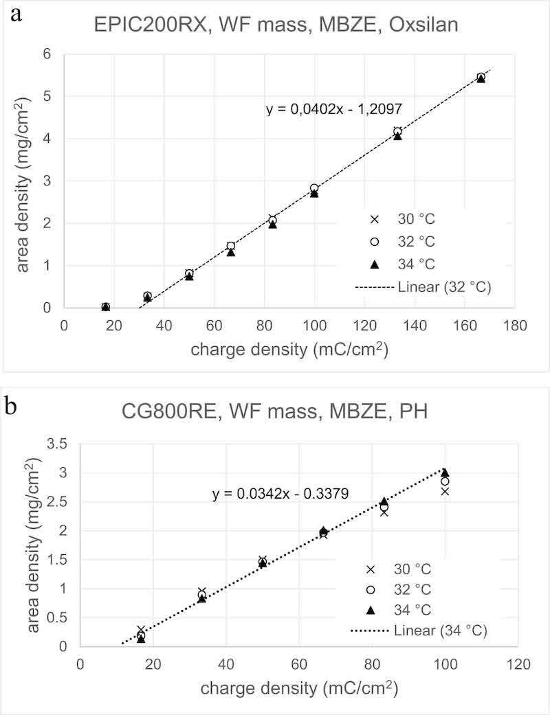
Fig. 5. Wet film mass area density in relation to the density of consumed charge for (a) EPIC200RX on Oxsilan pretreated MBZE panels, and (b) CG800RE on phosphated MBZE panels, with variation of deposition temperature.
3.1.2. Pretreatment
An influence of the substrate pretreatment is usually noticed when samples are compared that are coated with the same consumption of electrical charge, showing a higher deposited mass on phosphated panels than on thin film pretreated panels. The following graphs for both EC materials in Fig. 6 show that the slope of mass vs. charge for the different pretreatments is nearly identical for EPIC200RX and is reasonably similar for CG800RE. The charge threshold value is in the same range for both EC materials. The coagulation process, that is represented by the coulombic yield, seems not to depend on the pretreatment of the substrate for EPIC200RX but is slightly influenced by it for CG800RE.
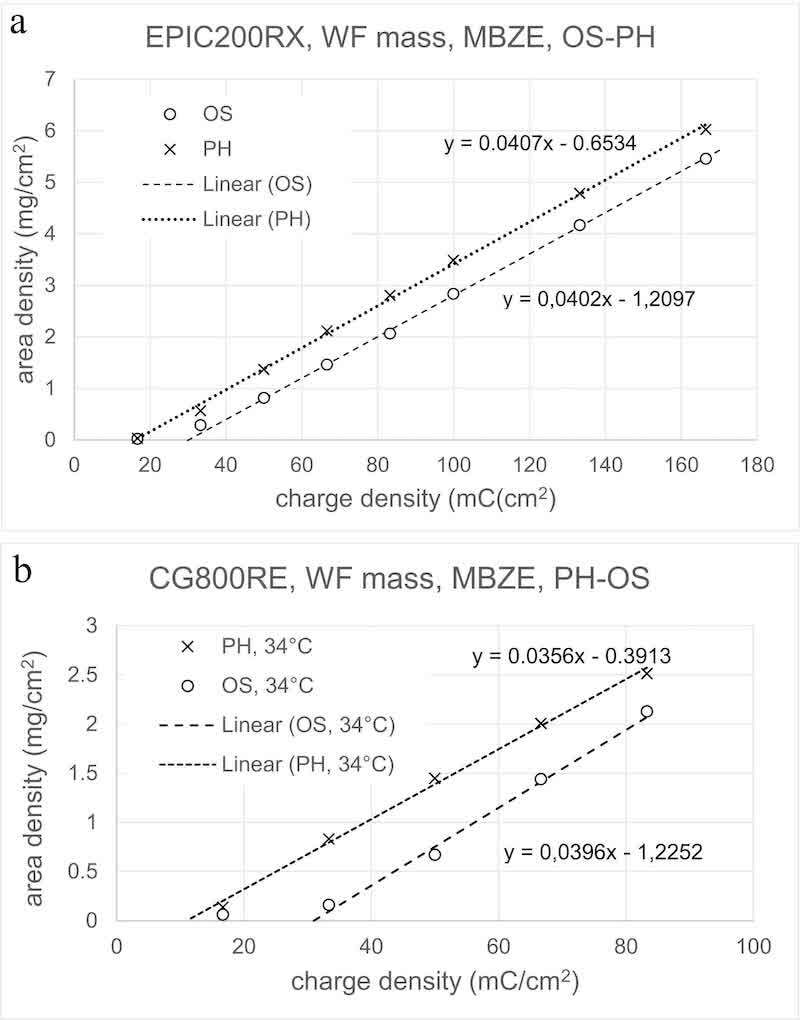
Fig. 6. WF mass area density in relation to charge density for phosphate and Oxsilan pretreated MBZE panels for (a) EPIC200RX and (b) CG800RE.
Table 1 shows the threshold values and the coulombic yield that are calculated from the linear regression of the graphs.
Table 1. Charge threshold density (mC/cm2) and coulombic yield for WF mass (C/g) on MBZE panels.
| Empty Cell | Charge threshold density (mC/cm2) | Coulombic yield (C/g) | ||
| EC material | Phosphate | Oxsilan | Phosphate | Oxsilan |
| EPIC200RX | 16.1 | 30.1 | 24.6 | 24.9 |
| CG800RE | 11.0 | 30.9 | 28.1 | 25.3 |
3.1.3. Substrate material
The influence of different substrate materials on coulombic yield and charge threshold is shown in Fig. 7 for EPIC200RX. The three substrate materials Aluminum, MBZE and MBS show a similar slope of mass vs. charge curves when the individual charge threshold is exceeded. Phosphated panels exhibit a smaller difference of threshold values than thin film pretreated panels.
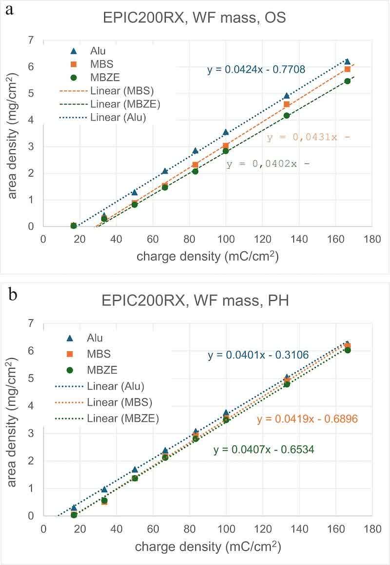
Fig. 7. WF mass area density in relation to charge density for MBZE, MBS, and Aluminum panels with EPIC200RX for (a) Oxsilan and (b) phosphate pretreatment.
Table 2 shows the threshold values and the coulombic yield that are calculated from the linear regression of the data points.
Table 2. Charge threshold density (mC/cm2) and coulombic yield for WF mass (C/g). MBZE panels, 32 °C, 500 rpm.
| EPIC200RX | Charge threshold density (mC/cm2) | Coulombic yield (C/g) | ||
| Substrate | Phosphate | Oxsilan | Phosphate | Oxsilan |
| Alu | 7.7 | 18.2 | 24.9 | 23.6 |
| MBZE | 16.1 | 30.1 | 24;6 | 24.9 |
| MBS | 16.5 | 28.8 | 23.9 | 23.2 |
Results of Aluminum and MBZE panels coated with CG800RE, presented in Fig. 8, do not differ significantly, neither in slope nor in charge threshold. Table 3 shows the coulombic yield and the calculated charge threshold for MBZE, exhibiting a clearly lower value for Phosphating than for Oxsilan.
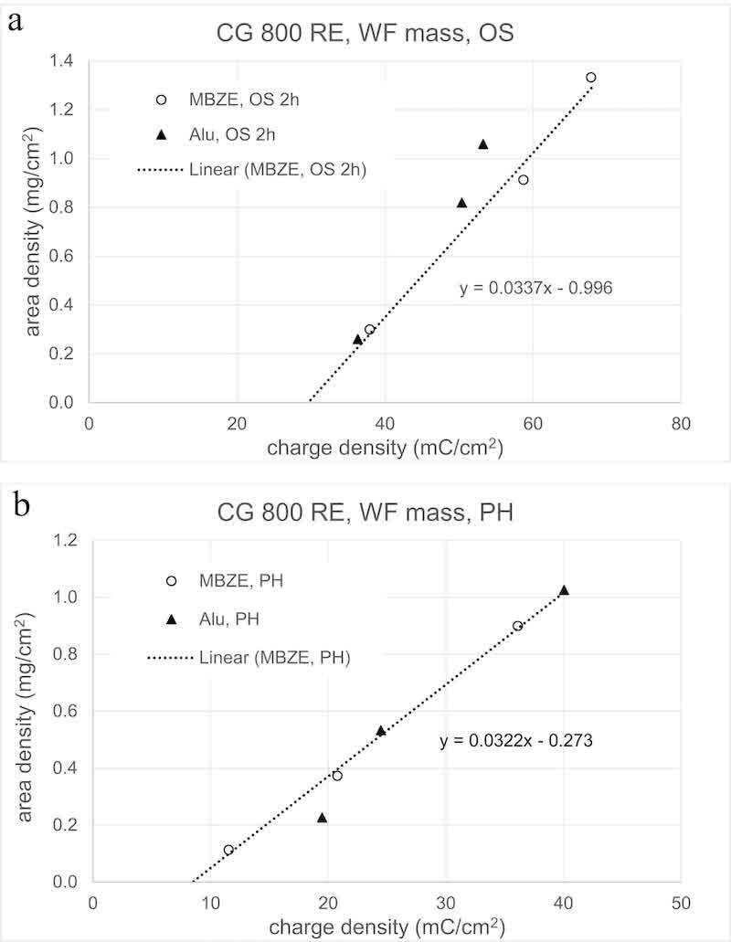
Fig. 8. WF mass area density in relation to charge density for MBZE and Aluminum panels with CG800RE for (a) Oxsilan and (b) phosphate pretreatment.
Table 3. Charge threshold density (mC/cm2) and coulombic yield for WF mass (C/g) with CG800RE. MBZE panels, 32 °C, 500 rpm.
{tabulizer:include style[rs_1vt85sq3.css] datatable[YToxOntzOjU6InRoZW1lIjtzOjk6ImxpZ2h0LmNzcyI7fQ==] css_files[rs_1vt85sq3.css] id[tab_I54MKM3KS9]}
| CG800RE | Charge threshold density (mC/cm2) | Coulombic yield (C/g) | ||
| Substrate | Phosphate | Oxsilan | Phosphate | Oxsilan |
| MBZE; Alu | 8.5 | 29.6 | 31.1 | 29.7 |
3.1.4. Current density
When deposition processes are compared that are carried out at different current densities, for EPIC200RX only a little influence on coulombic yield can be observed at values above 1 mA/cm2, visible by the similar gradients in Fig. 9(a) and (b). Up to at least 3 mA/cm2 the reaction rate is controlled by the current density. At values below 1 mA/cm2 a reduction of the coulombic yield is obvious. The charge thresholds decrease with increasing current density. For EPIC200RX the deposited mass at a given charge is higher for higher current density. A very high charge threshold occurs at a current density of 0.5 mA/cm2. For CG800RE there is no difference of coulombic yield and charge threshold between 1 and 2 mA/cm2 visible on phosphated MBZE panels.
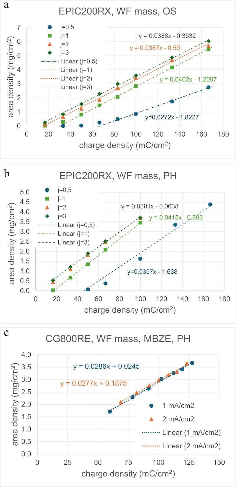
Fig. 9. WF mass area density in relation to charge density for different current densities for (a) EPIC200RX, Oxsilan, (b) EPIC200RX, phosphate, and (c) CG800RE, phosphate.
The values for coulombic yield and charge threshold in Table 4 are calculated from the linear regression of the data points in Fig. 9.
Table 4. Charge threshold density (mC/cm2) and coulombic yield for WF mass (C/g). EPIC200RX, MBZE panels, 32 °C, 500 rpm.
| EPIC200RX | Charge threshold density (mC/cm2) | Coulombic yield (C/g) | ||
| Curr. Dens. (mA/cm2) | Phosphate | Oxsilan | Phosphate | Oxsilan |
| 0.5 | 45.9 | 66.9 | 28.0 | 36.8 |
| 1 | 16.7 | 30.1 | 24.1 | 24.9 |
| 2 | 4.7 | 15.2 | 25.5 | 25.8 |
| 3 | 1.7 | 9.1 | 26.2 | 25.8 |
3.1.5. Flow velocity
A factor that is influencing the coulombic yield is the agitation of the bath. The rotation speed of the magnetic stirrer varies from 100 to 500 rpm, affecting the convection velocity of the electrolyte particles. Results for 2 different current densities are presented in Fig. 10 (a) and (b).
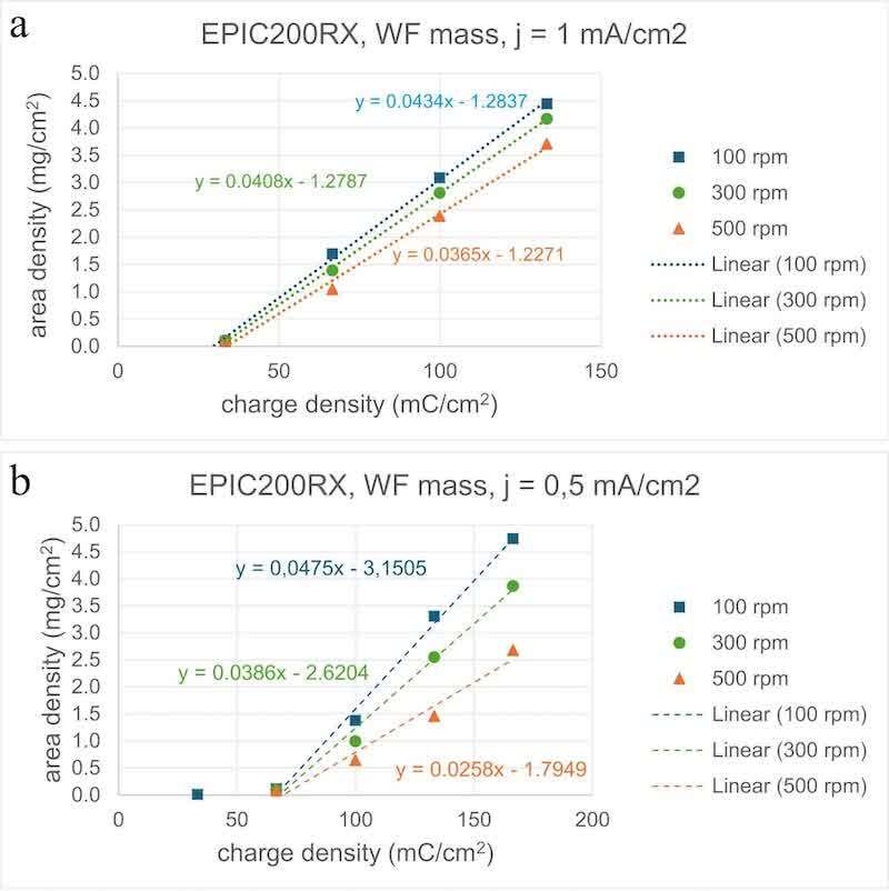
Fig. 10. WF mass area density in relation to charge density for EPIC200RX on Oxsilan -pretreated MBZE panels at different stirrer rotation speeds for (a) current density 1 mA/cm2 and (b) 0.5 mA/cm2.
The charge threshold is not influenced by the flow velocity. A similar behavior is obtained at 0.5 mA/cm2, but with generally lower yield, as can be expected from the former experiments. The dependence of coulombic yield on the rotational speed at 0.5 mA/cm2 is more distinct than at 1 mA/cm2. The calculated results for charge threshold and coulombic yield are presented in Table 5.
Table 5. Charge threshold density and coulombic yield for WF mass. MBZE panels, Oxsilan, 32 °C, EPIC200RX.
| EPIC200RX | Charge threshold density (mC/cm2) | Coulombic yield (C/g) | ||
| rotation (min−1) | 0.5 mA/cm2 | 1 mA/cm2 | 0.5 mA/cm2 | 1 mA/cm2 |
| 100 | 66.3 | 29.6 | 21.1 | 23.0 |
| 300 | 67.9 | 31.3 | 25.9 | 24.5 |
| 500 | 69.6 | 33.6 | 38.8 | 27.4 |
A flow simulation of the beaker and stirrer geometry showed a linear dependence of the flow velocity ranging from about 0.01 m/s to 0.1 m/s. Fig. 11 shows the simulated values for several distances to the cathode surface. These values are an approximation because the flow velocity is oscillating, and it is not homogeneous across the panel area.
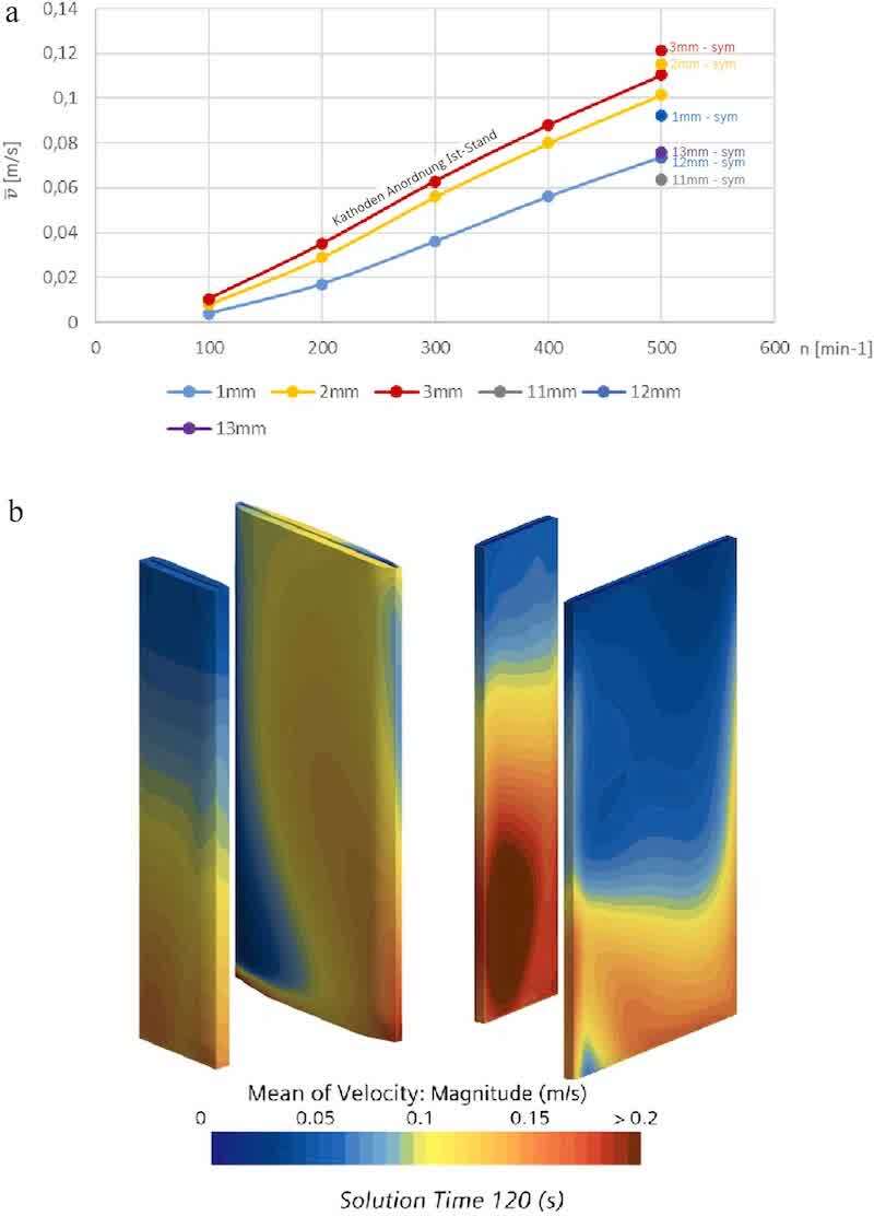
Fig. 11. Results of flow simulation of laboratory beaker. Flow velocity in relation to stirrer rotational speed (a), and velocity distribution on the test panel (broad rectangle) and the anode (thin rectangle) (b). Front and backside are displayed.
All presented values for the coulombic yield are given for the wet film mass. A reference value for the coulombic yield may be derived from titration of the paint with KOH. The consumed volume of the titrant at the equivalence point can be expressed corresponding to Faraday’s laws as a charge value and might be regarded as the minimum amount of electrolytic charge for the deposition. The exceeding amount of charge of an electrolytic deposition then indicates loss processes where ion current is not resulting in paint deposition. For CG800RE the titration equivalence value is about 36.4 C/g non-volatile (dry film) and the coulombic yield of the coating experiments varies between 38 and 45 C/g non-volatile (dry film).
3.2. Wet film resistance
The influence of several coating parameters on the wet film resistance is shown in the following evaluation of the coating experiments. The resistance results are evaluated in the constant current region (up to Umax). All Oxsilan pretreated panels have been dried in ambient climate for about 2–4 h prior to coating, if not stated otherwise. The resistance values are calculated using the recorded data of bath potential and current. The data of the bath potential sensor in front of the cathode is taken to exclude the bath resistance (US in Fig. 2). Even if this approach is not exact, the results are believed to be a good approximation. In the following graphs the product of wet film resistance multiplied by surface area is used for the y-axis to get transferable values for other panel sizes. This product can also be interpreted as resistivity times film thickness (see (Eq. 1)) and is denoted as “linear resistance”. Some groups of the same deposition charge are marked in some of the graphs to allow for an easier distinction between the influence of coulombic yield and film resistance. The spread of the mass area density within the groups represents the differences mainly of the charge threshold and secondly of the coulombic yield.
3.2.1. Temperature
The temperature dependency of the wet film resistance is displayed in the graphs of Fig. 12 for MBZE panels with Oxsilan pretreatment. Both EC materials show a similar curve shape, except for the distinctly higher resistance level of CG800RE. For very low deposited mass the film resistance is independent of bath temperature, but with increasing mass it becomes temperature dependent. At a given deposited mass, it is lower for higher bath temperature. The temperature induced resistance spread is smaller for EPIC200RX but distinctive for CG800RE.
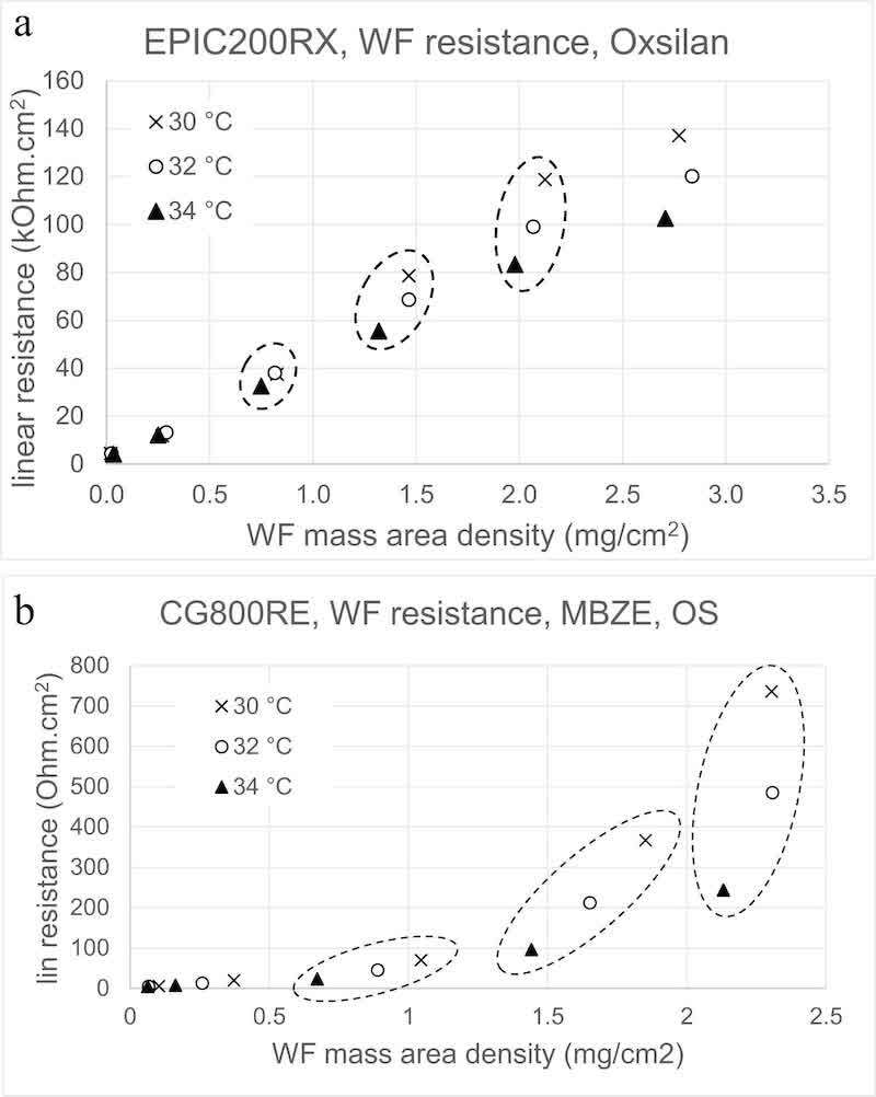
Fig. 12. Linear resistance in relation to the area density of wet film mass for EPIC200RX and CG800RE at different deposition temperatures.
3.2.2. Pretreatment
The pretreatment influences the wet film resistance, as the graphs in Fig. 13 (a) and (b) show for MBZE and for Aluminum panels at 32 °C with EPIC200RX. At a given deposited mass, the resistance of Oxsilan pretreated panels is always lower than that of phosphated panels, with the difference becoming larger at higher deposited mass. For EPIC200RX, the difference is more distinctive for Aluminum than for MBZE. For CG800RE the difference on MBZE is distinctive, as presented in Fig. 13 (c).
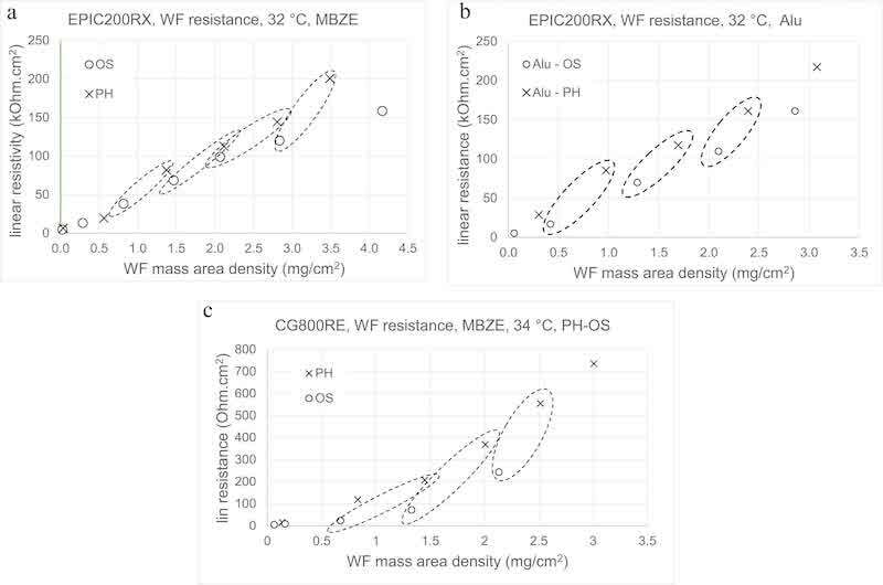
Fig. 13. Linear resistance in relation to the area density of wet film mass for EPIC200RX on Oxsilan-pretreated or phosphated (a) MBZE and (b) Aluminum panels. (c) CG800RE with Oxsilan-pretreated or phosphated MBZE panels.
3.2.3. Substrate material
A small influence of the substrate material is visible in the graphs of Fig. 14 for EPIC200RX, especially at higher deposited mass. The slightly higher resistance of Aluminum panels compared to MBZE and MBS panels is even more distinctive on phosphated panels than on Oxsilan pretreated panels.
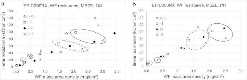
Fig. 14. Linear resistance in relation to the area density of wet film mass for EPIC200RX with (a) Oxsilan-pretreated panels or (b) phosphated panels of different substrate materials.
3.2.4. Current density
Fig. 15 shows coatings that have been carried out at different current densities. The graphs show a clear influence on wet film resistance on Oxsilan pretreated panels. With increasing current density, the resistance of the wet film at a given mass is decreasing. On phosphate panels this behavior is less significant and is observable only at higher deposited mass. Two groups of the same deposited charge are marked in the graphs. The experiments with 0.5 mA/cm2 have a very low deposited mass and are marked with a separate circle.
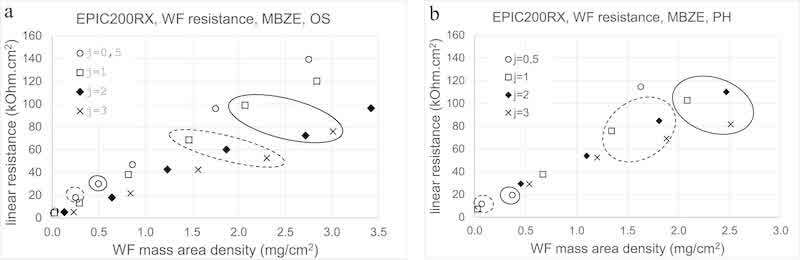
Fig. 15. Linear resistance in relation to the area density of wet film mass for Oxsilan-pretreated and phosphated MBZE panels coated with EPIC200RX at different current densities. The numbers are in mA/cm2.
3.2.5. Flow velocity
For EPIC200RX the agitation seems to have no significant effect on the wet film resistance of a given deposited mass. Fig. 16 shows graphs for current densities of 1 mA/cm2 and 0.5 mA/cm2.
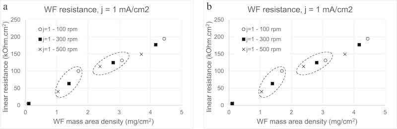
Fig. 16. Linear resistance in relation to the area density of wet film mass for Oxsilan-pretreated MBZE panels coated with EPIC200RX at different flow velocities at current densities of 0.5 and 1 mA/cm2.
3.2.6. PT aging
The graphs in Fig. 17 show the voltage curves and wet film resistance curves of Oxsilan pretreated panels, that have been aged for different periods of time prior to coating. The index “wiw” denotes the panels that have been coated directly after Oxsilan-PT without drying (wet in wet). “2 h” stands for 2 h and “7d” for 7 days aging. All coatings have been carried out at 32 °C with maximum current density set to 1 mA/cm2 and maximum voltage set to 260 V up to a total charge of 35 C for CG800RE and 37 C for EPIC200RX.
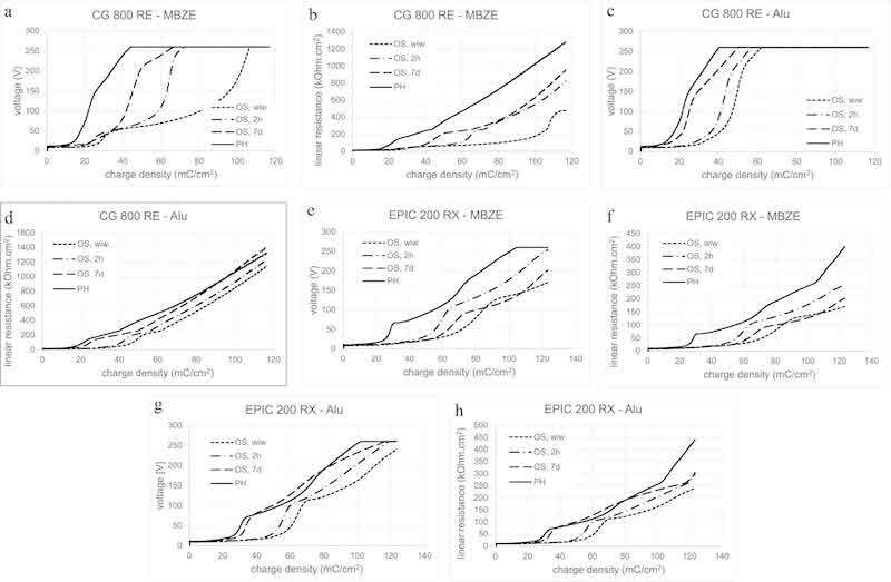
Fig. 17. Voltage and wet film resistance of CG800RE and EPIC200RX on Oxsilan-pretreated panels with different ageing.
The voltage curves are displayed in relation to the consumed charge. Up to the maximum voltage the electrical current is constant, and the voltage follows the wet film resistance. The maximum voltage is reached at a total resistance of 867 Ohm. Due to the linear relation between consumed charge and deposited mass (beyond the charge threshold), the nonlinearity of the voltage curves indicates a nonlinear relation between resistance and deposited mass.
Both EC materials show a significantly slower rise of voltage and correspondingly a slower rise of wet film resistance on MBZE panels at shorter pretreatment aging. On Aluminum panels these differences are not so distinctive. For comparison the curves of phosphated panels are also displayed, showing the fastest rise of wet film resistance on MBZE panels. On Aluminum panels the difference between 7 days aged Oxsilan and Phosphate is small. In general, the wet film resistance of EPIC200RX is increasing significantly slower than that of CG800RE.
3.2.7. Explanatory approach
The observation that a given deposited mass results in different resistance values depending on substrate material and its pretreatment is not self-explanatory. For homogeneous electron- or ion-conducting materials Ohm’s law is valid. With resistance R, resistivity ρ, conductor length d and area A it is:
R = ρd/A (1)
The linear resistance values in the graphs Fig. 12 to Fig. 16 are plotted in relation to the wet film mass area density. The volume density δ of a homogeneous material is the quotient of mass m and Volume V:
δ = m/V = m/dA (2)
Combining (Eq. 1) and (Eq. 2), the quotient of linear resistance RA divided by wet film mass area density m/A can be written as:
RA/m/A = ρd/ δd = ρ/δ (3)
which would be a constant value for a given homogeneous material of constant inner structure at a given temperature. Graphs of linear resistance in relation to mass area density would be linear with a constant slope independent of parameter variation.
For an inhomogeneous material consisting of two or more phases of different conductivity, the total values of ρ and δ will depend on the composition and inner structure of the heterogeneous mixture. If an equal mass of a given material that is deposited with different coating parameters results in different resistance values, a possible reason is the co-deposition of another phase with different conductivity.
3.3. 3D topography and structure of the wet film
The influence of several process parameters as well as of substrate material and its pretreatment on the structure and topography of the wet film was investigated by laser scanning microscope. The remains of hydrogen bubbles can clearly be seen in the wet film, prior to smoothing of the surface during the baking step. The following pictures show the 3D topography of the wet film at 200x magnification. The captured area has a width of about 0.5 mm and a lateral grid spacing of 50 µm.
3.3.1. Oxsilan aging
The following images in Fig. 18 show 3 Aluminum panels that have been coated with CG800RE at 32 °C and 500 rpm rotation for 180 s. The maximum voltage was set to 260 V and the maximum current density 1 mA/cm2. Table 6 shows the measured values for these panels.
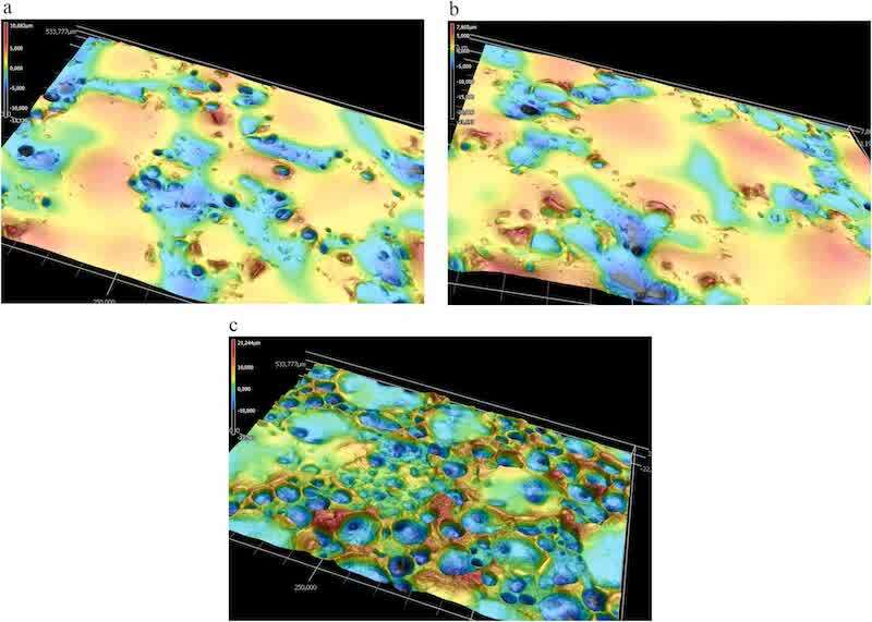
Fig. 18. Topography images of Aluminum panels coated with CG800RE at different Oxsilan ageing durations.
Table 6. Coating parameters of the images of Fig. 18.
| CG800RE | (a) | (b) | (c) |
| PT aging | wet in wet | 2 h | 14 days |
| charge density (mC/cm2) | 115 | 108 | 101 |
| WF lin. resistance (kOhm cm2) | 1012 | 1080 | 1311 |
Panels with pretreatment aging wet in wet and 2 h dried show very similar charge density and wet film resistance. Compared to these two panels, the panel with 14 days dried pretreatment has a slightly lower charge density but a significantly higher wet film resistance. It is significant in the 3D images that the first 2 panels exhibit a similar size and distribution of hydrogen bubbles, whereas the 14 days dried panel shows a higher density and smaller diameter.
3.3.2. Pretreatment
The influence of the pretreatment for Aluminum panels that have been either phosphated or Oxsilan coated is shown in Fig. 19. Images (a) and (b) show BASF CG800RE deposition, images (c) and (d) show PPG EPIC200RX deposition. The coating parameters were temperature 32 °C, agitation 500 rpm, and current density 1 mA/cm2. For both EC materials it is obvious that the phosphated panels exhibit a distinctively denser distribution of hydrogen bubbles than the Oxsilan coated panels. The diameter of the bubbles does not differ distinctively between phosphate and Oxsilan and is in a range of 10–30 µm. The difference of the wet film resistance between both pretreatments is large, especially for EPIC200RX. Table 7 shows the measured values for these panels.
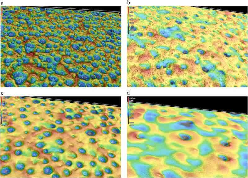
Fig. 19. Topography images of Aluminum panels coated with CG800RE: (a) phosphated and (b) Oxsilan pretreated; and for EPIC200RX: (c) phosphated and (d) Oxsilan pretreated.
Table 7. Coating parameters of the images of Fig. 19.
| Empty Cell | (a) | (b) | (c) | (d) |
| EC material | CG800RE | CG800RE | EPIC200RX | EPIC200RX |
| Pretreatment | Phosphate | Oxsilan | Phosphate | Oxsilan |
| charge density (mC/cm2) | 24.5 | 50.4 | 28.2 | 56.9 |
| WF mass area density (mg/cm2) | 0.53 | 0.82 | 0.64 | 0.7 |
| WF lin. resistance (kOhm cm2) | 69.6 | 71.2 | 55.3 | 22.2 |
| mass resistivity (kOhm/mg) | 131 | 87 | 86 | 32 |
The quotient of wet film resistance and wet film mass indicates the specific resistance that a wet film structure opposes to the ion current. This value is denominated as “mass resistivity” in this work. If the surface area is kept constant, this value correlates to the quotient of resistivity and volume density, ρ/δ. Different values obtained for the same EC material on the same area can be related to different structure and multi-phase composition of the coatings.
3.3.3. Current density
The images of Fig. 20 show MBZE panels with similar mass area density coated at 300 rpm but with different current densities. The sample with higher current density exhibits distinctively less hydrogen bubbles and smaller diameters. The difference of the wet film resistances is large, which corresponds well to the results shown in chapter 3.2. Table 8 shows the measurement results of these panels.
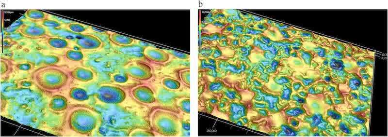
Fig. 20. Topography images of MBZE panels coated with EPIC200RX at different current densities.
Table 8. Coating parameters of the images of Fig. 20.
| EPIC200RX | (a) | (b) |
| current densities (mA/cm2) | 0.5 | 1 |
| charge density (mC/cm2) | 133 | 100 |
| DF thickness (µm) | 13.6 | 15.7 |
| DF mass area density (mg/cm2) | 2.1 | 2.3 |
| WF mass area density (mg/cm2) | 2.6 | 2.8 |
| WF lin. resistance (kOhm cm2) | 182 | 125 |
| mass resistivity (kOhm/mg) | 70 | 45 |
3.3.4. Flow velocity
Fig. 21 shows MBZE panels that have been coated with EPIC200RX at current density of 0,5 mA/cm2 but with 3 different rotation speeds. The panels possess comparable DF mass resp. DF thickness but the panel with the highest rotation speed exhibits a significant difference in size and number of hydrogen bubbles. Compared to 100 and 300 rpm, the size and number of bubbles is reduced. Along with it, mass resistivity also decreased. The measurement results are shown in Table 9.
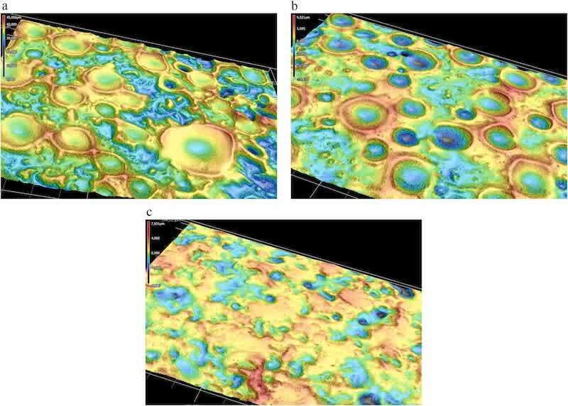
Fig. 21. Topography images of MBZE panels coated with EPIC200RX at different rotation speeds at current density 0.5 mA/cm2.
Table 9. Coating parameters of the images of Fig. 21.
| EPIC200RX | (a) | (b) | (c) |
| rotation speed (rpm) | 100 | 300 | 500 |
| charge density (mC/cm2) | 133 | 133 | 167 |
| DF thickness (µm) | 18.6 | 13.6 | 14.7 |
| WF thickness (µm) | 21.1 | 16.7 | 17 |
| DF mass area density (mg/cm2) | 2.7 | 2.1 | 2.2 |
| WF mass area density (mg/cm2) | 3.3 | 2.6 | 2.7 |
| WF lin. resistance (kOhm cm2) | 228 | 182 | 155 |
| mass resistivity (kOhm/mg) | 69 | 70 | 57 |
A similar decrease in size and number of hydrogen bubbles along with a decrease of the wet film resistance is occurring at MBZE panels that have been deposited with a charge density of 67 mC/cm2 at a current density of 1 mA/cm2. These topography images are displayed in Fig. 22. Here also the distribution of hydrogen bubbles is different in size and number. The coating parameters are shown in Table 10.
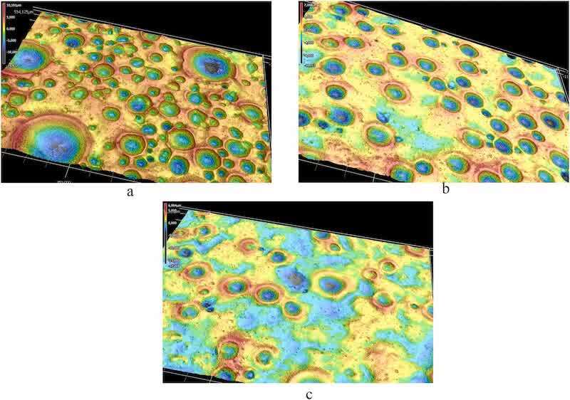
Fig. 22. Topography images of MBZE panels coated with EPIC200RX at different rotation speeds at current density 1 mA/cm2.
Table 10. Coating parameters of the images of Fig. 22.
| EPIC200RX | (a) | (b) | (c) |
| rotation speed (rpm) | 100 | 300 | 500 |
| charge density (mC/cm2) | 67 | 67 | 67 |
| DF thickness (µm) | 9.2 | 7.4 | 5.5 |
| DF mass area density (mg/cm2) | 1.4 | 1.1 | 0.8 |
| WF mass area density (mg/cm2) | 1.7 | 1.4 | 1.1 |
| WF lin. resistance (kOhm cm2) | 100 | 64 | 40 |
| mass resistivity (kOhm/mg) | 59 | 45 | 36 |
In Fig. 16, where the above results are grouped in the left circle, it can be noticed that at higher deposited mass the resistance is almost not dependent on rotation speed. Panels coated with a charge density of 100 mC/cm2, which are grouped in the right circle, show correspondingly a very similar topography.
3.4. Aging effect of Oxsilan
During the first seconds of the deposition process only a minimal area of the cathode is covered by EC material, and the value of the bath potential electrode represents the transfer resistance between substrate and electrolyte and the half-cell potentials. The transfer resistance is generated mainly by the pretreatment film and its ohmic part should depend on the current density. The graphs of Fig. 23 show the starting potential of MBZE and Aluminum panels at current densities of 1 and 2 mA/cm2. Three different aging conditions of Oxsilan pretreatment are compared to phosphate panels. On MBZE panels the values for wet in wet and 2 h dried panels are quite similar, but at 3 weeks drying a significant increase takes place, reaching a level comparable to phosphate. The values on Aluminum panels are generally higher and increase moderately, also reaching phosphate level after 3 weeks. The conformity of the results of both EC materials indicates that indeed the Oxsilan pretreatment causes the aging effect.
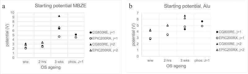
Fig. 23. Cathode potential sensor measurements at the beginning of the induction period vs. ageing of Oxsilan-pretreatment.
An estimation of the transfer resistance, roughly calculated from the potential values, results in about 2 Ohm for MBZE and 4 Ohm for Aluminum panels of 300 cm2 surface area, that have been dried for 2 h. The resistance rises to about 7 resp. 5 Ohm after 3 weeks. It is obvious that these very low resistances cannot account for the significant difference in the voltage curves of the coating process, when the wet film resistance increases to several hundred Ohm.
The aging effect can also be demonstrated by the contact angle of DI-water drops, with examples shown in Fig. 24 and Fig. 25. After 2 h drying in room air, the water drops still spread on MBZE surfaces resp. show a small angle on Aluminum panels. After 14 days of aging the contact angles increase to values of more than 70°. Phosphated panels aged in the same atmosphere don’t show this increase and exhibit still very low contact angles after long storing periods. An increase in the contact angle only occurs after baking.
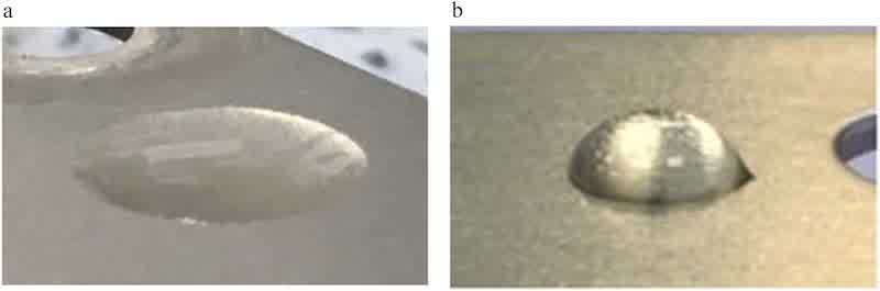
Fig. 24. Contact angle of DI water drops on Aluminum, Oxsilan pretreated: (a) aged 2 h; (b) aged 14 days.
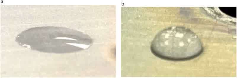
Fig. 25. Contact angle of DI water drops on MBZE, Oxsilan pretreated: (a) aged 2 h; (b) aged 14 days.
4. Discussion
The aim of this experimental work is to understand mode and magnitude of how several factors are influencing the two main parameters of the deposition process, coulombic yield and wet film resistance. The following Table 11 qualitatively illustrates the influence of the investigated factors on coulombic yield, charge threshold, and wet film resistance, as described in preceding former chapter.
Table 11. Factors experimentally influencing coulombic yield, charge threshold and wet film resistance. *) The increased coulombic yield at low current density is likely due to a geometric influence, with a possible explanation provided in the subsequent text.
| Empty Cell | Temp. | Pretreatm. | Substrate | Curr. dens. | Flow veloc. | PT Aging |
| Coul. yield | no | no | no | (no)*) | yes | - |
| Threshold | no | yes | yes | yes | no | - |
| Resistance | (yes) | yes | (yes) | yes | no | yes |
The factors influencing coulombic yield differ from those influencing charge threshold (resp. induction period). These two parameters are therefore considered to follow independent mechanisms. Charge threshold and wet film resistance share several influencing factors and could thus share some common mechanisms.
4.1. Induction period
A comparison of deposited mass and voltage in Fig. 26 shows that during the induction period, defined as the time until a steep rise of the deposition voltage is detected, no mass deposition is measurable within the scale’s resolution. The voltage rise, caused by increasing wet film resistance, is setting in synchronously with the measurable mass deposit. However, on panels with a charge density below the threshold, a light discoloration was already visible, even though no mass gain could be measured by a milligram scale. A minimal amount of resin was deposited, but at a very low deposition rate. The current value during the induction period is of the same amount as until the maximum voltage is reached; therefore, electrochemical electrode reactions occur, but without the effect of a significant film deposition. This observation could be explained by an electrode reaction during this period that does not result in deprotonation of the resin, respectively the production of hydroxide ions. The reduction of oxonium ions at the cathode (I) meets this condition, because it does not form OH--ions, and thus offers a possible explanation.
I. 2 H3O+ + 2 e- Û H2 + 2 H2O
II. 2 H2O + 2 e- Û H2 + 2 OH-
III. 2 H2O + O2 + 4 e- Û 4 OH-
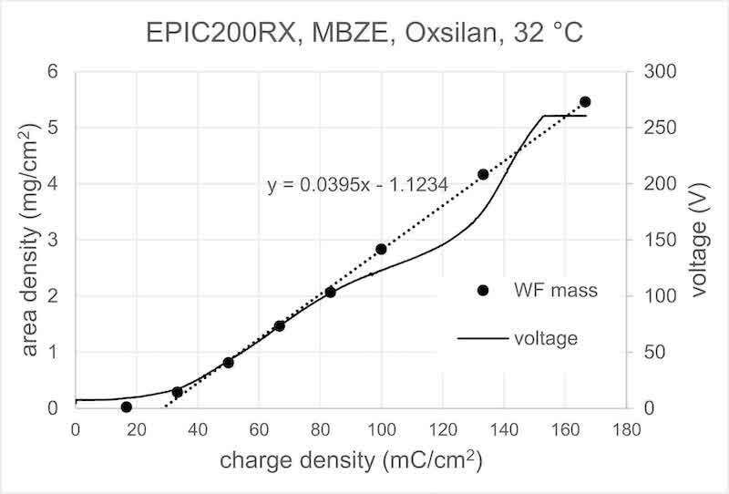
Fig. 26. Voltage and WF mass area density in relation to charge density for EPIC200RX on Oxsilan-pretreated MBZE panels.
The standard reduction potential of reaction (I) and reaction (II) at a given pH value is identical. In acidic electrolytes, reaction (I) is favored, while in basic electrolytes, reaction (II) is favored [4]. Given the acidic electrolyte in the beginning of the deposition process, it can be assumed that reaction (I) consumes a major part of the charge flow, thereby retarding the generation of hydroxide ions, resulting in a slow deposition rate of the resin film. The increase in pH due to the consumption of oxonium ions could gradually shift the charge flow towards reaction (II). Higher pH value also prevents the dissolution of precipitated resin. Variations in the degree of neutralization (DN) have been presented in [16], where an effect on the induction period was observed. At a DN of less than 100% almost no induction period was detected, but at 100% and above, it increased. The DN correlates with pH value, with an increase in oxonium ion concentration at DN > 100%.
However, the increase in pH value cannot explain the dependence of the induction period on substrate material and pretreatment. Differences in the film-building process that depend on these factors must therefore be considered. Experiments with current interruption, presented in [7], also showed that the induction period cannot be explained exclusively by concentration effects, but that irreversible changes to the substrate make a major contribution. The negligible impact of flow velocity on the charge threshold in Fig. 10 also indicates that the induction period is not influenced by convection, as a concentration-controlled process would be. The charge threshold in Table 11 is influenced mainly by substrate and PT type, factors that should not impact concentration. These findings are also described in [7]. These observations indicate a change of the PT film due to a charge induced reaction. A conversion reaction could be a cause for the induction period. A dependence of the composition of the thin-film pretreatment on the substrate material or the pretreatment process could influence a conversion reaction and thus affect the duration of the induction period.
The impact of current density on charge threshold could be related to geometric conditions of the laboratory setup. To destabilize the micelles, it is necessary to deprotonate a certain amount of the resin molecules. The reaction of the micelles with hydroxide ions takes place in the vicinity of the cathode. If, at high flow velocity and low current density, some micelles are only partly deprotonated and not destabilized, they will be reprotonated by the acid in the bulk electrolyte after leaving the cathode area. Externally, this would be observed as a charge loss, influencing both coulombic yield and charge threshold. Transferring this to an industrial production scale is difficult, because, on the one hand, the flow velocity, at least on the outer surface, is significantly higher (up to approx. 0.5 m/s), but on the other hand, the surfaces involved are also much larger. In internal areas and cavities, this effect would lead to a lower required amount of charge.
Phosphated surfaces and thin-film pretreated surfaces exhibit completely different structures, as displayed on Fig. 27. The phosphate layer consists of crystals of usually several µm diameter with narrow crevices in between. The phosphate crystals are non-conductive, leaving the bottom of the crevices as the only location for electrolysis. The cross-section available for ion transport is further reduced by the generation of hydrogen gas. In contrast, the Oxsilan surface, with a film thickness in the range of 100 nm, is electrically conductive. With an assumed coverage rate of more than 99% by the phosphate crystals [9], the current density in the crevices will be at least two orders of magnitude higher compared to Oxsilan pretreated substrates. The induction period will therefore be substantially shorter for these sites on the phosphated surface. The film will quickly start to grow at the crevices, causing a rapid increase in resistance, and spread over the non-conductive phosphate crystals. The nearly complete coverage of the substrate by non-conductive phosphate crystals also levels out the differences between substrate materials and surface conditions.
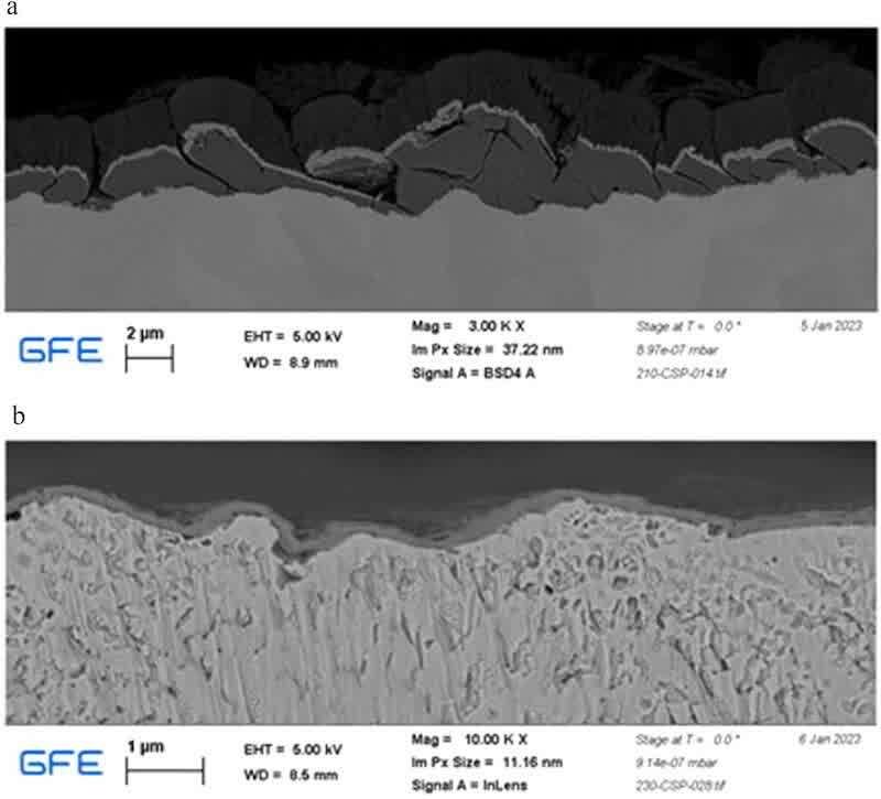
Fig. 27. SEM images of crosscuts of MBZE (a) phosphated and (b) Oxsilan pretreated.
4.2. Wet film resistance model
Two different models have been proposed in the literature to explain the localization of hydroxide ion generation during the deposition process and their transport to the electrolyte. In the first model, the porous film model (PF), electrolysis takes place at the bottom of pores that extend down to the metallic conductive substrate throughout the entire deposition process [2], [6], [14]. The ions move through these pores driven by the electrical field via electroosmosis.
In the second model, the IPFF model, hydroxide ions are generated by electrolysis of the water content of the wet film, occurring at the interface between pretreated substrate and wet film [10], [11]. One would infer from this model that the ions are accelerated by the electric field through the wet film and that the electrical resistance of the resin film is caused by the drag that it exerts on the migration of ions.
The results of the presented experiments for both examined EC materials exhibit distinct differences in wet film resistance, induced by several coating parameters. This feature contrasts with the deposition of a homogeneous film but could be explained by a second phase within the wet film having a different conductivity. This possible reason is explained in more detail at the end of chapter 3.2. Reduction of water at the cathode produces ½ mol of hydrogen gas per 1 mol of hydroxide ions, which will roughly deposit 3 kg or 2 liters of wet film of the examined EC materials. The volume of 1 mol hydrogen gas VH2 can be calculated by the ideal gas law with Temperature T, universal gas constant R and pressure p:
VH2 = RT/p (4)
Therefore, the hydrogen gas volume at 305 K and 1.013 bar of approximately 12.5 liters is about 6 times the volume of deposited EC material. The migration of ions will be hindered by the non-conductive hydrogen bubbles immersed in the wet film. The effect on resistance will depend on the bubble size and number, which corresponds well to the topography images of the wet film presented herein. The time that hydrogen bubbles remain in the wet film would also influence its resistance, with longer duration leading to an increased bubble quantity and thus increased resistance. A larger mobility of the bubbles at higher temperatures could explain the temperature dependence of the wet film resistance at higher film thickness that is presented in chapter 3.2. Assuming a temperature-dependent but time-invariant degassing rate of the wet film, in combination with the current-density-dependent generation rate of hydrogen, the hydrogen bubble saturation of the wet film would depend on the coating parameters. The addition of solvents enhancing the mobility of the hydrogen bubbles would possibly result in a reduction of wet film resistance. The effect of co-solvents on the trapping and the transition mobility of gas bubbles in low-Tg acrylic resins is described in [13], in addition to their influence on film formation.
The influence of modified hydrogen bubble size on film resistance by variation of the atmospheric pressure was presented in [15]. Buoyancy measurements of the hydrogen gas attached to the wet film are presented in [12]. We carried out experiments with clear, acidic and basic, electrolytes, where it was observed that hydrogen bubbles are larger and remain longer on an Oxsilan pretreated surface than on a phosphated surface. Differences were also observed between different substrate materials. A similar dependence of the adherence of hydrogen bubbles depending on surface conditions was described in [7]. Longer adherence time and larger size of hydrogen bubbles reduce the remaining metal surface area at the start of the deposition process and might contribute to the dependence of the induction time on the substrate material. On phosphated surfaces with a very small conductive area between the crystals, see Fig. 27, the hydrogen bubbles contribute to the fast increase in resistance.
The previously described porous film model would explain different wet film resistances by a different pore geometry. The experimental results of the sheet resistance presented here would mean following this model that high bath temperature and high current density lead to a pore geometry with less resistance, while the flow rate would have no influence on pore formation. Likewise, TFPT, especially with short aging, would lead to a pore geometry with higher resistance compared to phosphating. On MBZE and MBS substrates, the pore distribution would also exhibit lower resistance than on aluminum. Since the resolution of the scanning microscope is not sufficient to display small pores, this mechanism cannot be ruled out. However, considering the presented differences in the distribution of hydrogen bubbles, their contribution to the development of wet film resistance is assumed.
5. Conclusions
The EC deposition process is characterized mainly by two parameters: coulombic yield and wet film resistance. Several process factors can influence the evolution of these parameters during the deposition process. After the rollout of TFPT in the first automotive production plants it was observed that the extent of these factors’ influence is more distinct on TFPT than on customary phosphate PT. For future optimization of new PT and EC material developments, aiming at a more robust deposition process comparable to the conditions on phosphated cars, it is necessary to gain more knowledge on the extent of these factors.
The main difference between coating on TFPT and Phosphate lies in the evolution of wet film resistance. A possible explanation for this feature is presented in the size and amount of hydrogen bubbles that are immersed in the wet film. These bubbles alter the total resistance of the multi-phase film structure, and their varying distribution influences the local current density and thus the local coating thickness. For industrial coating, a uniform layer thickness growth on different substrates is desirable, meaning a uniform development of wet film resistance. Of the externally adjustable process parameters investigated here, only the current density has a significant effect in achieving this goal with thin-film pretreatment. The highest possible current density led to smaller differences. This results in requirements for the performance of the installed rectifiers.
Several process parameters have been examined, but future work must extend to, for example, material parameters like ash content or other process parameters like pH. The derivation of precise quantitative values requires a statistically more robust basis through the repetition of experiments. The quantitative deduction of the influencing factors from material parameters would enable target-oriented development. A better quantitative description of the mechanisms can additionally be used to deduce the algorithms of the film thickness simulation from material parameters.
Tobias Lux is with Mercedes-Benz AG, HPC L331, Sindelfingen D-71059, Germany
CRediT authorship contribution statement: Tobias Lux: Writing – original draft, Visualization, Validation, Supervision, Project administration, Methodology, Data curation, Conceptualization.
Declaration of Competing Interest: The authors declare that they have no known competing financial interests or personal relationships that could have appeared to influence the work reported in this paper.
Acknowledgment: The author wishes to thank itb Gmbh, Stuttgart, for carrying out flow velocity simulation of the beaker and the RWTH Aachen, GFE, for carrying out SEM and TEM analysis of phosphate and thin film pretreated samples.
References
1. A. Goldschmidt, H.-J. Streitberger, BASF-Handbuch Lackiertechnik, Vincentz, Hannover, 2002.
2. P.E. Pierce, The physical chemistry of the cathodic electrodeposition process, J. Coat. Technol. Res. 53 (1981) 52–67.
3. M.D. Maksimovi´ c, V.B. Miˇ skovi´ c-Stankovi´ c, N.V. Krstaji´ c, The effect of applied voltage on the cathodic electrodeposition process, Surf. Coat. Technol. 27 (1986) 89–94.
4. V.S. Bagotsky, Fundamentals of elechtrochemistry, J. Wiley & Sons, Hoboken, 2006.
5. F. Beck, Fundamental aspects of electrodeposition of paint, Prog. Org. Coat. 4 (1976) 1–60.
6. N.M. A´ camovi´ c, D.M. Draˇ zi´ c, V. B. Miˇ skovi´ c-Stankovi´ c, Influence of substrate on formation and growth Kinetics of cathodic electrocoat paint, Prog. Org. Coat. 25 (1995) 293–307.
7. F. Padash, B. Dorff, W. Liu, K. Ellwood, B. Okerberg, S.R. Zawacky, J.N. Harb, Characterization of initial film formation during cathodic electrodeposition of coatings, Prog. Org. Coat. 133 (2019) 395–405.
8. Y.-I. Suzuki, H. Fukui, K. Tsuchiya, Y.H. Ogata, Initiation Process of Film Formation for Cationic Electropaint System, Journ. Electrochem. Soc. 147 (10) (2000) 3700–3707.
9. W. Rausch, Die Phosphatierung von Metallen. E.G. Leuze, Bad Saulgau (2005).
10. Y.-I. Suzuki, H. Fukui, K. Tsuchiya, S. Arita, Y.H. Ogata, Correlation of Film Structure with Film Formation in Cationic Electropaint Systems, Journ. Electrochem. Soc. 150 (3) (2003) C115–C124.
11. Y.-I. Suzuki, H. Fukui, K. Tsuchiya, S. Arita, Y.H. Ogata, Effects of Resin Blend and Solvent on Film Formation Mechanism of Cationic Electropaint System, J. Electrochem. Soc. 150 (4) (2003) C251–C259.
12. H. Fobbe, R. Geueke, C. Wieners, Formation and detachment of gas bubbles during cathodic electrocoating: quantitative determination by means of buoyancy measurements, Prog. Org. Coat. 196 (2024) 1–9.
13. Z. Ranjbar, S. Rastegar, Influence of co-solvent content on electro-deposition behavior of acrylic lattices of different glass transition temperatures, Prog. Org. Coat. 57 (2006) 365–370.
14. V.B. Miˇ skovi´ c, M.D. Maksimovi´ c, The kinetics of organic film growth during the cathodic electrodeposition process, Surf. Technol. 26 (1985) 353–360.
15. G. San Jos´ e García, H. Fobbe, The influence of reduced pressures on the film formation of cathodic electrodeposition paints, Prog. Org. Coat. 104 (2017) 110–117.
16. Z. Ranjbar, S. Moradian, Characteristics and deposition behavior of epoxy-amine adducts in cathodic electrodeposition as a function of the degree of neutralization, Colloids Surf. A Physicochem. Eng. Asp. 219 (2003) 147–159.